|
|
|
PDF ICS9DB202 Data sheet ( Hoja de datos )
| Número de pieza | ICS9DB202 | |
| Descripción | Two 0.7V current mode differential HCSL output pairs | |
| Fabricantes | Integrated Circuit Systems | |
| Logotipo | ||
Hay una vista previa y un enlace de descarga de ICS9DB202 (archivo pdf) en la parte inferior de esta página. Total 11 Páginas | ||
|
No Preview Available !
www.DataSheet4U.com
Integrated
Circuit
Systems, Inc.
ICS9DB202
PCI EXPRESS™
JITTER ATTENUATOR
GENERAL DESCRIPTION
The ICS9DB202 is a high perfromance 1-to-2 Dif-
ICS ferential-to-HCSL Jitter Attenuator designed for use
HiPerClockS™ in PCI Express™ systems. In some PCI Express™
systems, such as those found in desktop PCs, the
PCI Express™ clocks are generated from a low
bandwidth, high phase noise PLL frequency synthesizer. In these
systems, a jitter-attenuating device may be necessary in order
to reduce high frequency random and deterministic jitter com-
ponents from the PLL synthesizer and from the system board.
The ICS9DB202 has two PLL bandwidth modes. In low band-
width mode, the PLL loop bandwidth is 500kHz.This setting of-
fers the best jitter attenuation and is still high enough to pass a
triangular input spread spectrum profile. In high bandwidth mode,
the PLL bandwidth is at 1MHz and allows the PLL to pass more
spread spectrum modulation.
For serdes which have x10 reference multipliers instead of x12.5
multipliers, each of the two PCI Express™ outputs (PCIEX0:1)
can be set for 125MHz instead of 100MHz by configuring the
appropriate frequency select pins (FS0:1).
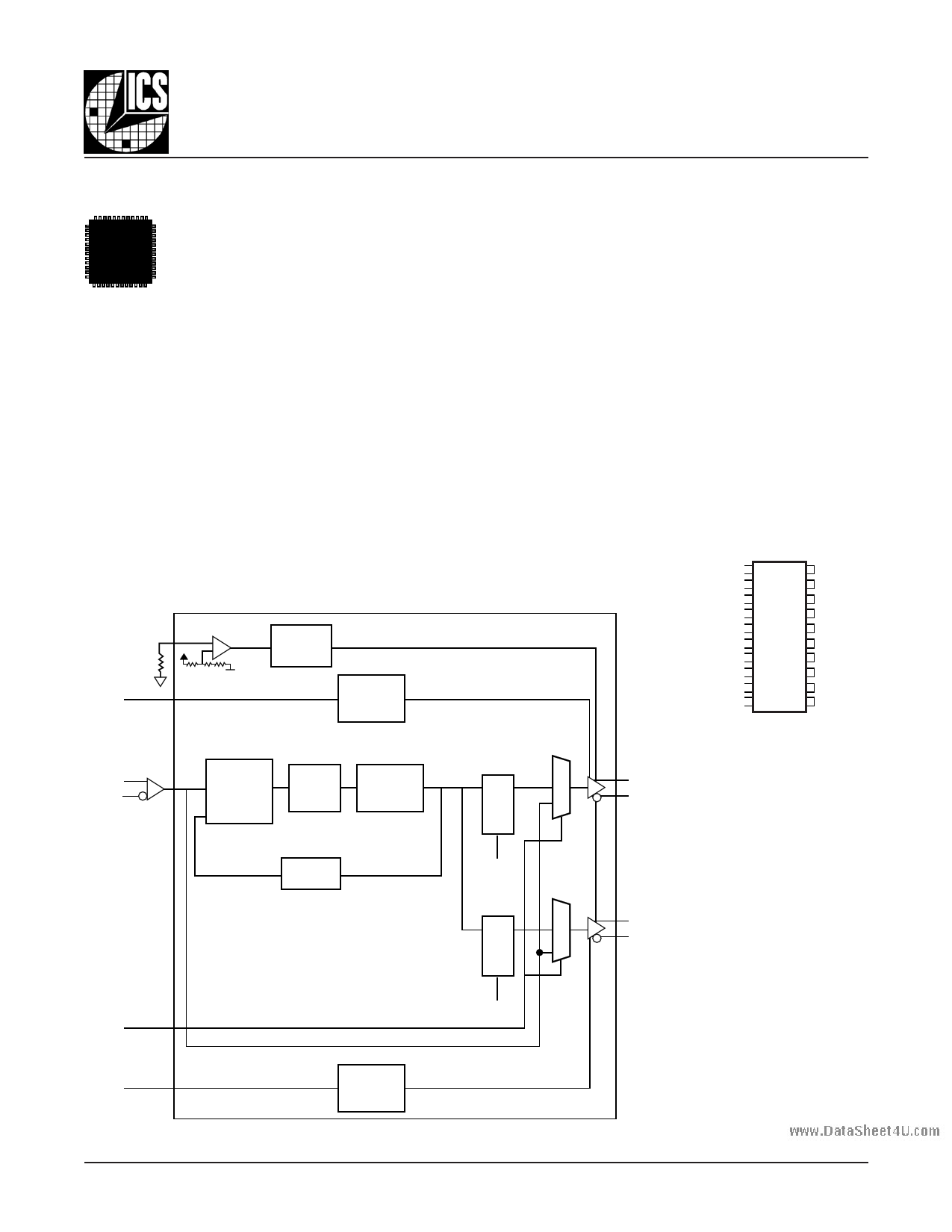
BLOCK DIAGRAM
IREF
+-
Current
Set
nOE0
1 HiZ
0 Enabled
nCLK
CLK
Phase
Detector
Loop
Filter
VCO
÷5
Internal Feedback
Features
• Two 0.7V current mode differential HCSL output pairs
• 1 differential clock input
• CLK and nCLK supports the following input types:
LVPECL, LVDS, LVHSTL, SSTL, HCSL
• Maximum output frequency: 140MHz
• Output skew: 110ps (maximum)
• Cycle-to-cycle jitter: 110ps (maximum)
• RMS phase jitter @ 100MHz, (1.5MHz - 22MHz):
2.42ps (typical)
• 3.3V operating supply
• 0°C to 70°C ambient operating temperature
• Lead-Free package available
• Industrial temperature information available upon request
PIN ASSIGNMENT
0
0 ÷4
1 ÷5 1
FS0
0 ÷5
1 ÷4
0
1
PLL_BW 1
2 0 VDDA
CLK 2 19 BYPASS
nCLK 3 18 IREF
FS0 4 17 FS1
VDD 5
16 VDD
GND 6 15 GND
PCIEXT0 7 14 PCIEXT1
PCIEXC0 8 13 PCIEXC1
VDD 9
12 VDD
nOE0 10 11 nOE1
ICS9DB202
20-Lead TSSOP
6.50mm x 4.40mm x 0.92
PCIEXT0
nPCIEXC0
package body
G Package
Top View
ICS9DB202
20-Lead, 209-MIL SSOP
5.30mm x 7.20mm x 1.75mm
body package
F Package
Top View
PCIEXT1
nPCIEXC1
BYPASS
nOE1
1 HiZ
0 Enabled
FS1
9DB202CG
DataSheet4 U .com
www.icst.com/products/hiperclocks.html
1
REV. A OCTOBER 6, 2004
1 page 
www.DataSheet4U.com
Integrated
Circuit
Systems, Inc.
0
-10
-20
-30
-40
-50
-60
-70
-80
-90
-100
-110
-120
-130
-140
-150
-160
-170
-180
-190
1k
TYPICAL PHASE NOISE AT 100MHZ
ICS9DB202
PCI EXPRESS™
JITTER ATTENUATOR
PCI Express™ Filter
100MHz
RMS Phase Jitter (Random)
1.5MHz to 22MHz = 2.42ps (typical)
Raw Phase Noise Data
Phase Noise Result by adding
PCI Express™ Filter to raw data
10k 100k 1M 10M 100M
OFFSET FREQUENCY (HZ)
The illustrated phase noise plot was taken using a low phase
noise signal generator, the noise floor of the signal generator is
less than that of the device under test.
Using this configuration allows one to see the true spectral purity
or phase noise performance of the PLL in the device under test.
Due to the tracking ability of a PLL, it will track the input signal
up to its loop bandwidth. Therefore, if the input phase noise is
greater than that of the PLL, it will increase the output phase
noise performance of the device. It is recommended that the
phase noise performance of the input is verified in order to
achieve the above phase noise performance.
9DB202CG
DataSheet4 U .com
www.icst.com/products/hiperclocks.html
5
REV. A OCTOBER 6, 2004
5 Page 
www.DataSheet4U.com
Integrated
Circuit
Systems, Inc.
TABLE 7. ORDERING INFORMATION
Part/Order Number
ICS9DB202CG
ICS9DB202CGT
ICS9DB202CGLF
ICS9DB202CGLFT
ICS9DB202CF
ICS9DB202CFT
ICS9DB202CFLF
ICS9DB202CFLFT
Marking
ICS9DB202CG
ICS9DB202CG
ICS9DB202CGL
ICS9DB202CGL
ICS9DB202CF
ICS9DB202CF
ICS9DB202CFLF
ICS9DB202CFLF
ICS9DB202
PCI EXPRESS™
JITTER ATTENUATOR
Package
20 Lead TSSOP
20 Lead TSSOP on Tape and Reel
20 Lead "Lead-Free" TSSOP
20 Lead "Lead-Free" TSSOP on
Tape and Reel
20 Lead SSOP
20 Lead SSOP on Tape and Reel
20 Lead "Lead-Free" SSOP
20 Lead "Lead-Free" SSOP on
Tape and Reel
Count
72 per Tube
2500
72 per Tube
2500
64 per Tube
1000
64 per Tube
1000
Temperature
0°C to 70°C
0°C to 70°C
0°C to 70°C
0°C to 70°C
0°C to 70°C
0°C to 70°C
0°C to 70°C
0°C to 70°C
The aforementioned trademarks, HiPerClockS™ and PCI Express™ iare trademarks of Integrated Circuit Systems, Inc. or its subsidiaries in the United States and/or other countries.
While the information presented herein has been checked for both accuracy and reliability, Integrated Circuit Systems, Incorporated (ICS) assumes no responsibility for either its use
or for infringement of any patents or other rights of third parties, which would result from its use. No other circuits, patents, or licenses are implied. This product is intended for use
in normal commercial applications. Any other applications such as those requiring extended temperature range, high reliability, or other extraordinary environmental requirements are
not recommended without additional processing by ICS. ICS reserves the right to change any circuitry or specifications without notice. ICS does not authorize or warrant any ICS
product for use in life support devices or critical medical instruments.
9DB202CG
www.icst.com/products/hiperclocks.html
REV. A OCTOBER 6, 2004
DataSheet4 U .com
11
11 Page | ||
| Páginas | Total 11 Páginas | |
| PDF Descargar | [ Datasheet ICS9DB202.PDF ] | |
Hoja de datos destacado
| Número de pieza | Descripción | Fabricantes |
| ICS9DB202 | Two 0.7V current mode differential HCSL output pairs | Integrated Circuit Systems |
| Número de pieza | Descripción | Fabricantes |
| SLA6805M | High Voltage 3 phase Motor Driver IC. |
Sanken |
| SDC1742 | 12- and 14-Bit Hybrid Synchro / Resolver-to-Digital Converters. |
Analog Devices |
|
DataSheet.es es una pagina web que funciona como un repositorio de manuales o hoja de datos de muchos de los productos más populares, |
| DataSheet.es | 2020 | Privacy Policy | Contacto | Buscar |