|
|
|
PDF MC74LVXT4051 Data sheet ( Hoja de datos )
| Número de pieza | MC74LVXT4051 | |
| Descripción | ANALOG MULTIPLEXER DEMULTIPLEXER HIGH-PERFORMANCE SILICON-GATE CMOS | |
| Fabricantes | ON Semiconductor | |
| Logotipo | ||
Hay una vista previa y un enlace de descarga de MC74LVXT4051 (archivo pdf) en la parte inferior de esta página. Total 16 Páginas | ||
|
No Preview Available !
www.DataSheet4U.com
MC74LVXT4051
Analog Multiplexer/
Demultiplexer
High–Performance Silicon–Gate CMOS
The MC74LVXT4051 utilizes silicon–gate CMOS technology to
achieve fast propagation delays, low ON resistances, and low leakage
currents. This analog multiplexer/demultiplexer controls analog
voltages that may vary across the complete power supply range (from
VCC to VEE).
The LVXT4051 is similar in pinout to the LVX8051, the HC4051A,
and the metal–gate MC14051B. The Channel–Select inputs determine
which one of the Analog Inputs/Outputs is to be connected, by means
of an analog switch, to the Common Output/Input. When the Enable
pin is HIGH, all analog switches are turned off.
The Channel–Select and Enable inputs are compatible with standard
TTL levels. These inputs are over–voltage tolerant (OVT) for level
translation from 6.0 V down to 3.0 V.
This device has been designed so the ON resistance (RON) is more
linear over input voltage than the RON of metal–gate CMOS analog
switches and High–Speed CMOS analog switches.
• Select Pins Compatible with TTL Levels
• Fast Switching and Propagation Speeds
• Low Crosstalk Between Switches
• Analog Power Supply Range (VCC – VEE) = *3.0 V to )3.0 V
• Digital (Control) Power Supply Range (VCC – GND) = 2.5 to 6.0 V
• Improved Linearity and Lower ON Resistance Than Metal–Gate,
HSL, or VHC Counterparts
• Low Noise
• Designed to Operate on a Single Supply with VEE = GND, or Using
Split Supplies up to $ 3.0 V
• Break–Before–Make Circuitry
http://onsemi.com
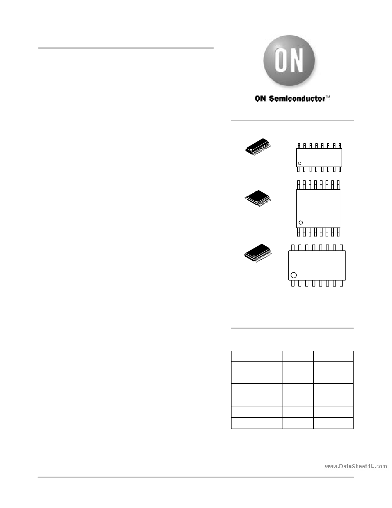
SO–16
D SUFFIX
CASE 751B
TSSOP–16
DT SUFFIX
CASE 948F
MARKING DIAGRAMS
16 9
LVXT4051
AWLYYWW
18
16 9
LVXT
4051
AWLYWW
18
16
SO EIAJ–16
M SUFFIX
CASE 966
1
LVXT4051
ALYW
A
L, WL
Y, YY
W, WW
= Assembly Location
= Wafer Lot
= Year
= Work Week
9
8
ORDERING INFORMATION
Device
Package
Shipping
MC74LVXT4051D
SO–16
48 Units/Rail
MC74LVXT4051DR2
SO–16 2500 Units/Reel
MC74LVXT4051DT TSSOP–16 96 Units/Rail
MC74LVXT4051DTR2 TSSOP–16 2500 Units/Reel
MC74LVXT4051M
SO EIAJ–16 48 Units/Rail
MC74LVXT4051MEL SO EIAJ–16 2000 Units/Reel
© Semiconductor Components Industries, LLC, 2002
January, 2002 – Rev. 3
DataSheet4 U .com
1
Publication Order Number:
MC74LVXT4051/D
1 page 
www.DataSheet4U.com
MC74LVXT4051
AC CHARACTERISTICS (CL = 50 pF, Input tr = tf = 3 ns)
Guaranteed Limit
Symbol
Parameter
VCC
V
VEE
V
*55 to 25°C
Min Typ Max
v85°C
Min Max
tPLH,
tPHL
Maximum Propagation Delay,
Channel–Select to Analog
Output
(Figures 16 and 17)
2.5 0
3.0 0
4.5 0
3.0 *3.0
40 45
28 30
23 25
23 25
tPLZ,
tPHZ
Maximum Propagation Delay,
Enable to Analog Output (Fig-
ures 14 and 15)
2.5 0
3.0 0
4.5 0
3.0 *3.0
40 45
28 30
23 25
23 25
tPZL,
tPZH
Maximum Propagation Delay,
Enable to Analog Output (Fig-
ures 14 and 15)
2.5 0
3.0 0
4.5 0
3.0 *3.0
40 45
28 30
23 25
23 25
v125°C
Min Max
50
35
30
28
50
35
30
28
50
35
30
28
Unit
ns
ns
ns
Typical @ 25°C, VCC = 5.0 V, VEE = 0V
CPD Power Dissipation Capacitance (Figure 18) (Note 7)
45
CIN Maximum Input Capacitance, Channel–Select or Enable Inputs
10
CI/O Maximum Capacitance
(All Switches Off)
Analog I/O
Common O/I
Feedthrough
10
10
1.0
7. Used to determine the no–load dynamic power consumption: PD = CPD VCC2f + ICC VCC.
pF
pF
pF
ADDITIONAL APPLICATION CHARACTERISTICS (GND = 0 V)
Symbol
Parameter
Condition
Typ
VCC
VEE
V V 25°C Unit
BW Maximum On–Channel
Bandwidth or Minimum
Frequency Response
VIS = ½ (VCC – VEE)
Ref and Test Attn = 10 dB
Source Amplitude = 0 dB
(Figure 7)
3.0 0.0 80 MHz
4.5 0.0 80
6.0 0.0 80
3.0 *3.0 80
VISO
Off–Channel Feedthrough
Isolation
f = 1 MHz; VIS = ½ (VCC – VEE)
Adjust Network Analyzer output to 10 dBm on each
3.0
4.5
0.0 *70 dB
0.0 *70
output from the power splitter.
6.0 0.0 *70
(Figures 8 and 9)
3.0
*3.0
*70
VONL
Maximum Feedthrough
On Loss
VIS = ½ (VCC – VEE)
Adjust Network Analyzer output to 10 dBm on each
3.0
4.5
0.0 *2 dB
0.0 *2
output from the power splitter.
6.0 0.0 *2
(Figure 11)
3.0
*3.0
*2
Q Charge Injection
VIN = VCC to VEE, fIS = 1 kHz, tr = tf = 3 ns
RIS = 0 W, CL= 1000 pF, Q = CL * ∆VOUT
(Figure 10)
5.0 0.0 9.0 pC
3.0 *3.0 12
THD
Total Harmonic Distortion
THD + Noise
fIS = 1 MHz, RL = 10 KW, CL = 50 pF,
VIS = 5.0 VPP sine wave
VIS = 6.0 VPP sine wave
(Figure 19)
%
6.0 0.0 0.10
3.0
*3.0
0.05
DataSheet4 U .com
http://onsemi.com
5
5 Page 
www.DataSheet4U.com
MC74LVXT4051
APPLICATIONS INFORMATION
The Channel Select and Enable control pins should be at
VCC or GND logic levels. VCC being recognized as a logic
high and GND being recognized as a logic low. In this
example:
VCC = )5 V = logic high
GND = 0 V = logic low
The maximum analog voltage swing is determined by the
supply voltages VCC and VEE. The positive peak analog
voltage should not exceed VCC. Similarly, the negative peak
analog voltage should not go below VEE. In this example,
the difference between VCC and VEE is five volts. Therefore,
using the configuration of Figure 21, a maximum analog
signal of five volts peak–to–peak can be controlled. Unused
analog inputs/outputs may be left floating (i.e., not
connected). However, tying unused analog inputs and
outputs to VCC or GND through a low value resistor helps
minimize crosstalk and feedthrough noise that may be
picked up by an unused switch.
Although used here, balanced supplies are not a
requirement. The only constraints on the power supplies are
that:
VEE – GND = 0 to *6 volts
VCC – GND = 2.5 to 6 volts
VCC – VEE = 2.5 to 6 volts
and VEE v GND
When voltage transients above VCC and/or below VEE are
anticipated on the analog channels, external Germanium or
Schottky diodes (Dx) are recommended as shown in
Figure 22. These diodes should be able to absorb the
maximum anticipated current surges during clipping.
)3.0 V
*3.0 V
ANALOG
SIGNAL
)3.0 V
16
ANALOG
ON SIGNAL
)3.0 V
)5 V
*3.0 V
GND
ANALOG
SIGNAL
)5 V
16
ANALOG
ON SIGNAL
)5 V
GND
*3.0 V
6 11
7 10
89
TO EXTERNAL CMOS
CIRCUITRY 0 to 3.0 V
DIGITAL SIGNALS
Figure 20. Application Example
6 11 TO EXTERNAL CMOS
7 10 CIRCUITRY 0 to 5 V
8 9 DIGITAL SIGNALS
Figure 21. Application Example
VCC
Dx
Dx
VEE
VEE
VCC
16
ON/OFF
VCC
Dx
Dx
VEE
7
8
Figure 22. External Germanium or Schottky Clipping Diodes
DataSheet4 U .com
http://onsemi.com
11
11 Page | ||
| Páginas | Total 16 Páginas | |
| PDF Descargar | [ Datasheet MC74LVXT4051.PDF ] | |
Hoja de datos destacado
| Número de pieza | Descripción | Fabricantes |
| MC74LVXT4051 | ANALOG MULTIPLEXER DEMULTIPLEXER HIGH-PERFORMANCE SILICON-GATE CMOS | ON Semiconductor |
| MC74LVXT4051 | ANALOG MULTIPLEXER DEMULTIPLEXER HIGH-PERFORMANCE SILICON-GATE CMOS | ON Semiconductor |
| MC74LVXT4052 | Analog Multiplexer / Demultiplexer | ON Semiconductor |
| MC74LVXT4053 | Analog Multiplexer/ Demultiplexer | ON Semiconductor |
| Número de pieza | Descripción | Fabricantes |
| SLA6805M | High Voltage 3 phase Motor Driver IC. |
Sanken |
| SDC1742 | 12- and 14-Bit Hybrid Synchro / Resolver-to-Digital Converters. |
Analog Devices |
|
DataSheet.es es una pagina web que funciona como un repositorio de manuales o hoja de datos de muchos de los productos más populares, |
| DataSheet.es | 2020 | Privacy Policy | Contacto | Buscar |