|
|
|
PDF K2723 Data sheet ( Hoja de datos )
| Número de pieza | K2723 | |
| Descripción | MOSFET ( Transistor ) - 2SK2723 | |
| Fabricantes | NEC | |
| Logotipo | ||
Hay una vista previa y un enlace de descarga de K2723 (archivo pdf) en la parte inferior de esta página. Total 8 Páginas | ||
|
No Preview Available !
DATA SHEET
MOS Field Effect Power Transistors
2SK2723
SWITCHING
N-CHANNEL POWER MOS FET
INDUSTRIAL USE
DESCRIPTION
This product is N-Channel MOS Field Effect Transistor
www.DataSheet4dUe.sciogmned for high current switching spplications.
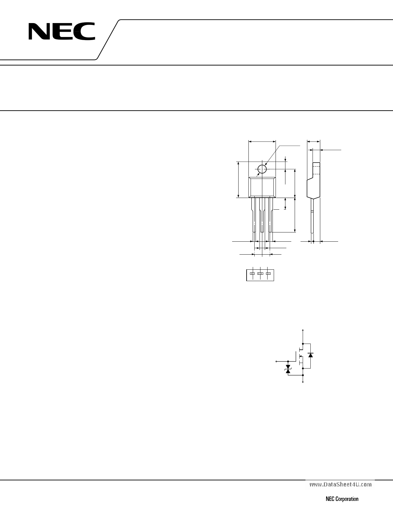
PACKAGE DIMENSIONS
(in millimeter)
10.0 ± 0.3
4.5 ± 0.2
3.2 ± 0.2
2.7 ± 0.2
FEATURES
• Low On-Resistance
RDS (on) 1 = 40mΩ Max. (VGS = 10 V, ID = 13 A)
RDS (on) 2 = 60mΩ Max. (VGS = 4 V, ID = 13 A)
• Low Ciss Ciss = 830 pF Typ.
• Built-in G-S Protection Diode
• Isolated TO-220 Package
0.7 ± 0.1
2.54
1.3 ± 0.2
1.5 ± 0.2
2.54
2.5 ± 0.1
0.65 ± 0.1
123
1.Gate
2.Drain
3.Source
MP-45F (ISOLATED TO-220)
ABSOLUTE MAXIMUM RATINGS (TA = 25 °C)
Drain to Source Voltage
VDSS
60
Gate to Source Voltage
VGSS
±20
Drain Current (DC)
ID (DC)
±25
Drain Current (pulse)*
ID (pulse)
±100
Total Power Dissipation (TA = 25 °C) PT
2.0
Total Power Dissipation (Tc = 25 °C) PT
25
Channel Temperature
Tch 150
Storage Temperature
Tstg −55 to +150
*PW ≤ 10 µs, Duty Cycle ≤ 1%
V
V
A
A
W
W
°C
°C
Drain
Gate
Body
Diode
Gate Protection
Diode
Source
The diode connected between the gate and source of the transistor serves as a protector against ESD. When this
deveice acutally used, an addtional protection circiut is externally required if voltage exceeding the rated voltage
may be applied to this device.
The information in this document is subject to change without notice.
Document No. D10623EJ2V0DS00 (2nd edition)
Date Published April 1996 P
Printed in Japan
© 1994
1 page 
2SK2723
DRAIN TO SOURCE ON-STATE RESISTANCE vs.
CHANNEL TEMPERATURE
80
60 VGS=4V
40
VGS=10V
20
www.DataSheet4U.com
0
ID = 13A
- 50 0 50 100 150
Tch - Channel Temperature -°C
10 000
CAPACITANCE vs. DRAIN TO
SOURCE VOLTAGE
VGS = 0
f = 1 MHz
1 000
100
Ciss
Coss
Crss
10
0.1
1 10
VDS - Drain to Source Voltage - V
100
1 000
REVERSE RECOVERY TIME vs.
DIODE CURRENT
di/dt =100A/µs
VGS = 0
100
10
1
0.1 1 10 100
IF - Dionde Current - A
SOURCE TO DRAIN DIODE
FORWARD VOLTAGE
Pulsed
100
VGS=10V
10
VGS=0
1
0.1
0
0.5 1.0
VSD - Source to Drain Voltage - V
1.5
1 000
100
10
SWITCHING CHARACTERISTICS
tr
tf
td(off)
td(on)
VDD =30V
VGS =10V
1 RG =10Ω
0.1 1 10 100
ID - Drain Current - A
DYNAMIC INPUT/OUTPUT CHARACTERISTICS
80 16
ID = 25A
14
60 VGS 12
VDD=12V
40 30V
48V
10
8
6
20 4
VDS 2
0
0 10 20 30 40
QG - Gate Charge - nC
5
5 Page | ||
| Páginas | Total 8 Páginas | |
| PDF Descargar | [ Datasheet K2723.PDF ] | |
Hoja de datos destacado
| Número de pieza | Descripción | Fabricantes |
| K2723 | MOSFET ( Transistor ) - 2SK2723 | NEC |
| K2725 | MOSFET ( Transistor ) - 2SK2725 | Renesas Technology |
| Número de pieza | Descripción | Fabricantes |
| SLA6805M | High Voltage 3 phase Motor Driver IC. |
Sanken |
| SDC1742 | 12- and 14-Bit Hybrid Synchro / Resolver-to-Digital Converters. |
Analog Devices |
|
DataSheet.es es una pagina web que funciona como un repositorio de manuales o hoja de datos de muchos de los productos más populares, |
| DataSheet.es | 2020 | Privacy Policy | Contacto | Buscar |