|
|
|
PDF VO2611 Data sheet ( Hoja de datos )
| Número de pieza | VO2611 | |
| Descripción | (VO2601 - VO2631) High Speed Optocoupler | |
| Fabricantes | Vishay Intertechnology | |
| Logotipo | ||
Hay una vista previa y un enlace de descarga de VO2611 (archivo pdf) en la parte inferior de esta página. Total 12 Páginas | ||
|
No Preview Available !
6N137, VO2601, VO2611, VO2630, VO2631, VO4661
www.vishay.com
Vishay Semiconductors
High Speed Optocoupler, Single and Dual, 10 MBd
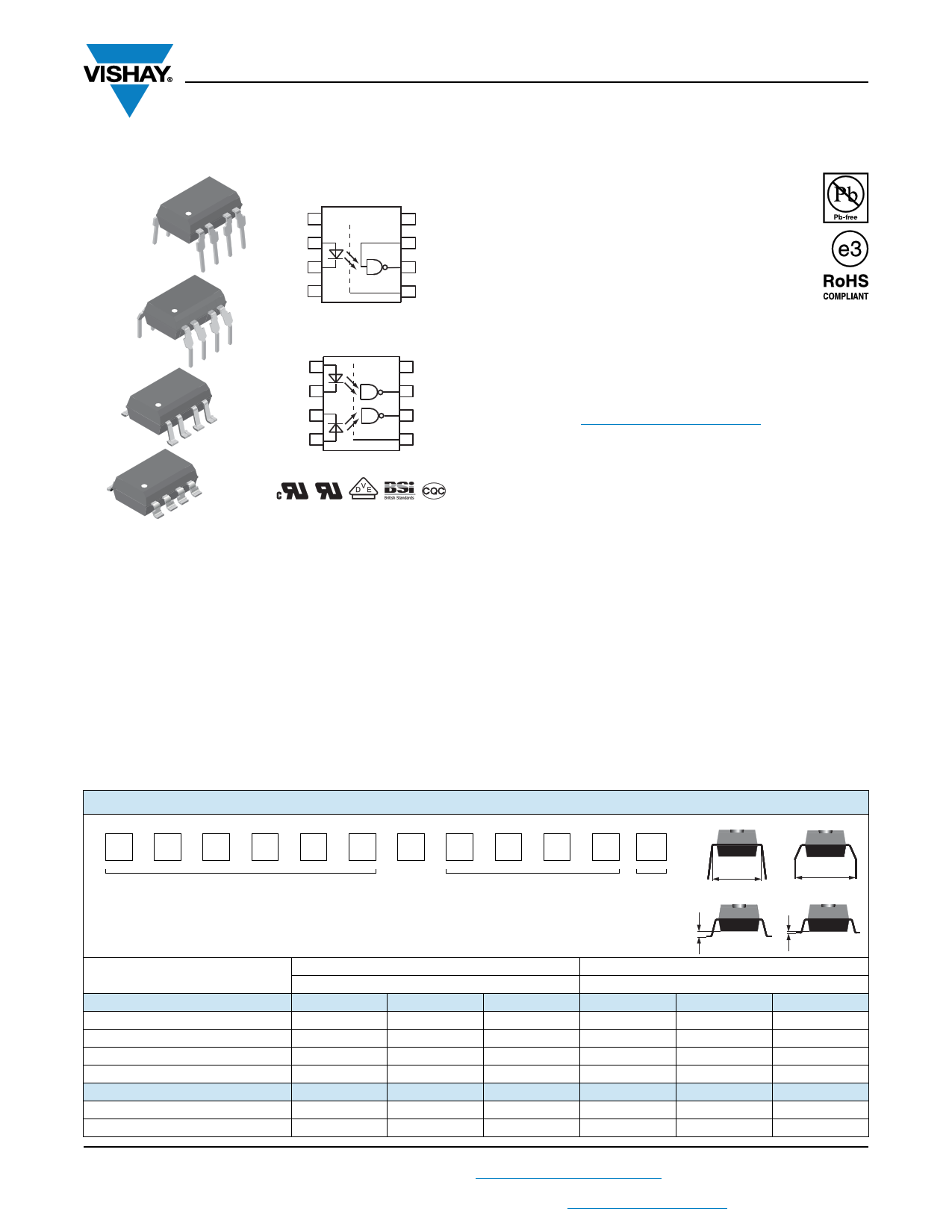
Single channel
NC 1
A2
C3
NC 4
8 VCC
7 VE
6 VO
5 GND
6N137, VO2601, VO2611
Dual channel
A1 1
C1 2
C2 3
A2 4
8 VCC
7 VO1
6 VO2
5 GND
VO2630, VO2631, VO4661
22747
DESCRIPTION
The 6N137, VO2601, and VO2611 are single channel
10 MBd optocouplers utilizing a high efficient input LED
coupled with an integrated optical photodiode IC detector.
The detector has an open drain NMOS-transistor output,
providing less leakage compared to an open collector
Schottky clamped transistor output. The VO2630, VO2631,
and VO4661 are dual channel 10 MBd optocouplers. For the
single channel type, an enable function on pin 7 allows the
detector to be strobed. The internal shield provides a
guaranteed common mode transient immunity of 5 kV/μs for
the VO2601 and VO2631 and 15 kV/μs for the VO2611 and
VO4661. The use of a 0.1 μF bypass capacitor connected
between pin 5 and 8 is recommended.
FEATURES
• Choice of CMR performance of 15 kV/μs,
5 kV/μs, and 1000 V/μs
• High speed: 10 MBd typical
• +5 V CMOS compatibility
• Pure tin leads
• Guaranteed AC and DC performance over
temperature: -40 °C to +100 °C temperature
range
• Meets IEC 60068-2-42 (SO2) and IEC 60068-2-43 (H2S)
requirements
• Low input current capability of 5 mA
• Material categorization: for definitions of compliance
please see www.vishay.com/doc?99912
APPLICATIONS
• Microprocessor system interface
• PLC, ATE input/output isolation
• Computer peripheral interface
• Digital fieldbus isolation: CC-link, DeviceNet, profibus, SDS
• High speed A/D and D/A conversion
• AC plasma display panel level shifting
• Multiplexed data transmission
• Digital control power supply
• Ground loop elimination, noise isolation
AGENCY APPROVALS
• UL1577
• cUL
• DIN EN 60747-5-5 (VDE 0884-5) available with option 1
• BS EN 60950-1
• CQC GB8898-2011, GB4943.1-2011
ORDERING INFORMATION
V O 2 6 0 1 - X 0 # #T
PART NUMBER
PACKAGE OPTION
TAPE
AND
REEL
DIP-8
7.62 mm
Option 7
Option 6
10.16 mm
Option 9
AGENCY CERTIFIED/PACKAGE
BSI, UL, cUL
DIP-8
DIP-8, 400 mil, option 6
SMD-8, option 7
SMD-8, option 9
VDE, BSI, UL, cUL
DIP-8, 400 mil, option 6
SMD-8, option 7
1000
6N137
6N137-X006
6N137-X007T
6N137-X009T
1000
-
-
CHANNELS 1
CMR (V/μs)
5000
VO2601
VO2601-X006
VO2601-X007T
-
5000
VO2601-X016
VO2601-X017T
15 000
VO2611
VO2611-X006
VO2611-X007T
-
15 000
VO2611-X016
VO2611-X017T
1000
VO2630
VO2630-X006
VO2630-X007T
VO2630-X009T
1000
-
-
> 0.7 mm
CHANNELS 2
CMR (V/μs)
5000
VO2631
VO2631-X006
VO2631-X007T
-
5000
VO2631-X016
VO2631-X017T
> 0.1 mm
15 000
VO4661
VO4661-X006
VO4661-X007T
-
15 000
-
-
Rev. 1.9, 16-Mar-15
1 Document Number: 84732
For technical questions, contact: [email protected]
THIS DOCUMENT IS SUBJECT TO CHANGE WITHOUT NOTICE. THE PRODUCTS DESCRIBED HEREIN AND THIS DOCUMENT
ARE SUBJECT TO SPECIFIC DISCLAIMERS, SET FORTH AT www.vishay.com/doc?91000
1 page 
6N137, VO2601, VO2611, VO2630, VO2631, VO4661
www.vishay.com
Vishay Semiconductors
IF
B
A
VFF
VCC
Single channel
1 VCC 8
VE
27
VOUT
36
45
GND
VCM
+-
Pulse generator
ZO = 50 Ω
RL
Output VO
0.1 µF monitoring
bypass node
VCM 0 V
VCM (PEAK)
Switch AT A: IF = 0 mA
VO 5 V
VO (min.)
Switch AT A: IF = 7.5 mA
VO 0.5 V
VO (max.)
CMH
CML
18976-2
Fig. 4 - Single Channel Test Circuit for Common Mode Transient Immunity
IF
B
A
VFF
Dual channel
1 VCC 8
27
36
VCC
RL Output VO
monitoring
0.1 µF node
bypass
18977-1
45
GND
VCM
+-
Pulse generator
ZO = 50 Ω
Fig. 5 - Dual Channel Test Circuit for Common Mode Transient Immunity
SAFETY AND INSULATION RATINGS
PARAMETER
Climatic classification (according to IEC 68 part 1)
Comparative tracking index
Rated isolation voltage
Maximum transient isolation voltage
Maximum repetitive peak isolation voltage
Isolation resistance
Output safety power
Input safety current
Input safety temperature
Creepage distance
Clearance distance
Creepage distance
Clearance distance
Insulation thickness, reinforced rated
TEST CONDITION
SYMBOL
t = 1 min
VIO = 500 V, Tamb = 25 °C
VIO = 500 V, Tamb = 100 °C
Standard DIP-4
Standard DIP-4
400 mil DIP-4
400 mil DIP-4
per BSI 60950
CTI
VISO
VIOTM
VIORM
RIO
RIO
PSO
ISI
TSI
DTI
VALUE
40/100/21
175
5300
8000
890
≥ 1012
≥ 1011
500
300
175
≥8
≥8
≥8
≥8
≥ 0.4
UNIT
VRMS
V
V
Ω
Ω
mW
mA
°C
mm
mm
mm
mm
mm
Note
• As per IEC 60747-5-5, § 7.4.3.8.2, this optocoupler is suitable for “safe electrical insulation” only within the safety ratings. Compliance with
the safety ratings shall be ensured by means of protective circuits.
Rev. 1.9, 16-Mar-15
5 Document Number: 84732
For technical questions, contact: [email protected]
THIS DOCUMENT IS SUBJECT TO CHANGE WITHOUT NOTICE. THE PRODUCTS DESCRIBED HEREIN AND THIS DOCUMENT
ARE SUBJECT TO SPECIFIC DISCLAIMERS, SET FORTH AT www.vishay.com/doc?91000
5 Page 
6N137, VO2601, VO2611, VO2630, VO2631, VO4661
www.vishay.com
Vishay Semiconductors
PACKAGE MARKING (example of VO2601-X017T)
VO2601
V YWW 68
Notes
• VDE logo is only marked on option 1 parts.
• Tape and reel suffix (T) is not part of the package marking.
SOLDER PROFILES
300
5s
250 235 °C to
260 °C
200
first wave
wave
ca. 200 K/s
150
100 °C to
130 °C
100
Lead temperature
second
wave
ca. 2 K/s
full line: typical
dotted line:
process limits
2 K/s
ca. 5 K/s
50 forced cooling
0
0
94 8626
50 100 150 200 250
Time (s)
Fig. 24 - Wave Soldering Double Wave Profile According to
J.STD-020 for DIP-8 Devices
HANDLING AND STORAGE CONDITIONS
ESD level: HBM class 2
Floor life: unlimited
Conditions: Tamb < 30 °C, RH < 85 %
Moisture sensitivity level 1, according to J-STD-020
300
250 255 °C
240 °C
217 °C
200
max. 260 °C
245 °C
max. 30 s
150
max. 120 s
max. 100 s
100
max. ramp down 6 °C/s
50 max. ramp up 3 °C/s
0
0
19841
50 100 150 200 250 300
Time (s)
Fig. 25 - Lead (Pb)-free Reflow Solder Profile According to
J-STD-020 for SMD-8 Devices
Rev. 1.9, 16-Mar-15
11 Document Number: 84732
For technical questions, contact: [email protected]
THIS DOCUMENT IS SUBJECT TO CHANGE WITHOUT NOTICE. THE PRODUCTS DESCRIBED HEREIN AND THIS DOCUMENT
ARE SUBJECT TO SPECIFIC DISCLAIMERS, SET FORTH AT www.vishay.com/doc?91000
11 Page | ||
| Páginas | Total 12 Páginas | |
| PDF Descargar | [ Datasheet VO2611.PDF ] | |
Hoja de datos destacado
| Número de pieza | Descripción | Fabricantes |
| VO2611 | (VO2601 - VO2631) High Speed Optocoupler | Vishay Intertechnology |
| VO2611 | High Speed Optocoupler | Vishay Siliconix |
| Número de pieza | Descripción | Fabricantes |
| SLA6805M | High Voltage 3 phase Motor Driver IC. |
Sanken |
| SDC1742 | 12- and 14-Bit Hybrid Synchro / Resolver-to-Digital Converters. |
Analog Devices |
|
DataSheet.es es una pagina web que funciona como un repositorio de manuales o hoja de datos de muchos de los productos más populares, |
| DataSheet.es | 2020 | Privacy Policy | Contacto | Buscar |