|
|
|
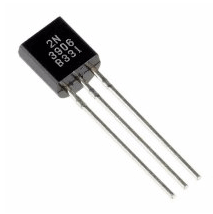
PDF 2N3906 Data sheet ( Hoja de datos )
| Número de pieza | 2N3906 | |
| Descripción | (2N3905 / 2N3906) General Purpose Transistors | |
| Fabricantes | Motorola Semiconductors | |
| Logotipo | ||
 1. -40V, PNP Transistor - KEC Hay una vista previa y un enlace de descarga de 2N3906 (archivo pdf) en la parte inferior de esta página. Total 6 Páginas | ||
|
No Preview Available !
MOTOROLA
SEMICONDUCTOR TECHNICAL DATA
Order this document
by 2N3905/D
General Purpose Transistors
PNP Silicon
COLLECTOR
3
2
BASE
1
EMITTER
MAXIMUM RATINGS
Rating
Symbol
Value
Unit
Collector – Emitter Voltage
Collector – Base Voltage
Emitter – Base Voltage
Collector Current — Continuous
Total Device Dissipation @ TA = 25°C
Derate above 25°C
VCEO
VCBO
VEBO
IC
PD
40 Vdc
40 Vdc
5.0 Vdc
200 mAdc
625 mW
5.0 mW/°C
Total Power Dissipation @ TA = 60°C
Total Device Dissipation @ TC = 25°C
Derate above 25°C
PD
PD
250 mW
1.5 Watts
12 mW/°C
Operating and Storage Junction
Temperature Range
TJ, Tstg – 55 to +150
°C
THERMAL CHARACTERISTICS(1)
Characteristic
Symbol
Max
Unit
Thermal Resistance, Junction to
Ambient
RqJA 200 °C/W
Thermal Resistance, Junction to Case
RqJC
83.3
°C/W
ELECTRICAL CHARACTERISTICS (TA = 25°C unless otherwise noted)
Characteristic
OFF CHARACTERISTICS
Collector – Emitter Breakdown Voltage (2)
(IC = 1.0 mAdc, IB = 0)
Collector – Base Breakdown Voltage
(IC = 10 mAdc, IE = 0)
Emitter – Base Breakdown Voltage
(IE = 10 mAdc, IC = 0)
Base Cutoff Current
(VCE = 30 Vdc, VEB = 3.0 Vdc)
Collector Cutoff Current
(VCE = 30 Vdc, VEB = 3.0 Vdc)
1. Indicates Data in addition to JEDEC Requirements.
v v2. Pulse Test: Pulse Width 300 ms; Duty Cycle 2.0%.
Preferred devices are Motorola recommended choices for future use and best overall value.
REV 2
Motorola Small–Signal Transistors, FETs and Diodes Device Data
© Motorola, Inc. 1996
2N3905
2N3906*
*Motorola Preferred Device
1
2
3
CASE 29–04, STYLE 1
TO–92 (TO–226AA)
Symbol
Min
V(BR)CEO
V(BR)CBO
V(BR)EBO
IBL
ICEX
40
40
5.0
—
—
Max Unit
— Vdc
— Vdc
— Vdc
50 nAdc
50 nAdc
1
1 page 
TYPICAL STATIC CHARACTERISTICS
2N3905 2N3906
2.0
TJ = +125°C
1.0 +25°C
0.7
– 55°C
0.5
0.3
0.2
VCE = 1.0 V
0.1
0.1
1.0
0.2 0.3
0.5 0.7 1.0
2.0 3.0
5.0 7.0 10
IC, COLLECTOR CURRENT (mA)
Figure 13. DC Current Gain
0.8
IC = 1.0 mA
0.6
10 mA
30 mA
0.4
20 30
50 70 100
200
TJ = 25°C
100 mA
0.2
0
0.01
0.02 0.03 0.05 0.07 0.1
0.2 0.3
0.5 0.7 1.0
IB, BASE CURRENT (mA)
Figure 14. Collector Saturation Region
2.0 3.0
5.0 7.0 10
1.0
TJ = 25°C
0.8
0.6
VBE(sat) @ IC/IB = 10
VBE @ VCE = 1.0 V
0.4
VCE(sat) @ IC/IB = 10
0.2
0
1.0 2.0 5.0 10
20
50 100 200
IC, COLLECTOR CURRENT (mA)
Figure 15. “ON” Voltages
1.0
0.5 qVC FOR VCE(sat)
0
– 0.5
– 1.0
– 1.5 qVB FOR VBE(sat)
+25°C TO +125°C
– 55°C TO +25°C
+25°C TO +125°C
– 55°C TO +25°C
– 2.0
0
20 40 60 80 100 120 140 160 180 200
IC, COLLECTOR CURRENT (mA)
Figure 16. Temperature Coefficients
Motorola Small–Signal Transistors, FETs and Diodes Device Data
5
5 Page | ||

| Páginas | Total 6 Páginas | |
| PDF Descargar | [ Datasheet 2N3906.PDF ] | |
Hoja de datos destacado
| Número de pieza | Descripción | Fabricantes |
| 2N3902 | HIGH VOLTAGE NPN SILICON TRANSISTORS | Boca Semiconductor Corporation |
| 2N3902 | Bipolar Transistor | Multicomp |
| 2N3902 | NPN HIGH POWER SILICON TRANSISTOR | Microsemi |
| 2N3902 | Bipolar NPN Device | Seme LAB |
| Número de pieza | Descripción | Fabricantes |
| SLA6805M | High Voltage 3 phase Motor Driver IC. |
Sanken |
| SDC1742 | 12- and 14-Bit Hybrid Synchro / Resolver-to-Digital Converters. |
Analog Devices |
|
DataSheet.es es una pagina web que funciona como un repositorio de manuales o hoja de datos de muchos de los productos más populares, |
| DataSheet.es | 2020 | Privacy Policy | Contacto | Buscar |