|
|
|
PDF OV2640 Data sheet ( Hoja de datos )
| Número de pieza | OV2640 | |
| Descripción | Color CMOS UXGA (2.0 MegaPixel) CAMERACHIP | |
| Fabricantes | OmniVision Technologies | |
| Logotipo | ||
1. OV2640 Hay una vista previa y un enlace de descarga de OV2640 (archivo pdf) en la parte inferior de esta página. Total 30 Páginas | ||
|
No Preview Available !
Omni
ision
®
Advanced Information
Preliminary Datasheet
OV2640 Color CMOS UXGA (2.0 MegaPixel) CAMERACHIPTM
with OmniPixel2TM Technology
General Description
The OV2640 CAMERACHIPTM is a low voltage CMOS image
sensor that provides the full functionality of a single-chip
UXGA (1632x1232) camera and image processor in a small
footprint package. The OV2640 provides full-frame,
sub-sampled, scaled or windowed 8-bit/10-bit images in a
wide range of formats, controlled through the Serial Camera
Control Bus (SCCB) interface.
This product has an image array capable of operating at up
to 15 frames per second (fps) in UXGA resolution with
complete user control over image quality, formatting and
output data transfer. All required image processing functions,
including exposure control, gamma, white balance, color
saturation, hue control, white pixel canceling, noise
canceling, and more, are also programmable through the
SCCB interface. The OV2640 also includes a compression
engine for increased processing power. In addition,
OmniVision CAMERACHIPS use proprietary sensor technology
to improve image quality by reducing or eliminating common
lighting/electrical sources of image contamination, such as
fixed pattern noise, smearing, etc., to produce a clean, fully
stable color image.
Note: The OV2640 uses a lead-free
Pb package.
Features
• High sensitivity for low-light operation
• Low operating voltage for embedded portable apps
• Standard SCCB interface
• Output support for Raw RGB, RGB (RGB565/555),
GRB422, YUV (422/420) and YCbCr (4:2:2) formats
• Supports image sizes: UXGA, SXGA, SVGA, and any
size scaling down from SXGA to 40x30
• VarioPixel® method for sub-sampling
• Automatic image control functions including Automatic
Exposure Control (AEC), Automatic Gain Control
(AGC), Automatic White Balance (AWB), Automatic
Band Filter (ABF), and Automatic Black-Level
Calibration (ABLC)
• Image quality controls including color saturation,
gamma, sharpness (edge enhancement), lens
correction, white pixel canceling, noise canceling, and
50/60 Hz luminance detection
• Line optical black level output capability
• Video or snapshot operation
• Zooming, panning, and windowing functions
• Internal/external frame synchronization
• Variable frame rate control
• Supports LED and flash strobe mode
• Supports scaling
• Supports compression
• Embedded microcontroller
Ordering Information
Product
OV02640-VL9A (Color, lead-free)
Package
38-pin CSP2
Applications
• Cellular and Camera Phones
• Toys
• PC Multimedia
• Digital Still Cameras
Key Specifications
Array Size
UXGA 1600 x 1200
Core 1.2VDC + 5%
Power Supply
Analog 2.5 ~ 3.0VDC
I/O 1.7V to 3.3V
Power
Requirements
125 mW (for 15 fps, UXGA
Active
YUV mode)
140 mW (for
15
fps,
UXGA
compressed mode)
Standby 600 µA
Temperature Operation -30°C to 70°C
Range Stable Image 0°C to 50°C
• YUV(422/420)/YCbCr422
Output
Formats
(8-bit)
•
•
RGB565/555
8-bit compressed data
• 8-/10-bit Raw RGB data
Lens Size 1/4"
Chief Ray Angle 25° non-linear
Maximum UXGA/SXGA 15 fps
Image
SVGA 30 fps
Transfer Rate
CIF 60 fps
Sensitivity 0.6 V/Lux-sec
S/N Ratio 40 dB
Dynamic Range 50 dB
Scan Mode Progressive
Maximum Exposure Interval 1247 x tROW
Gamma Correction Programmable
Pixel Size 2.2 µm x 2.2 µm
Dark Current 15 mV/s at 60°C
Well Capacity 12 Ke
Fixed Pattern Noise <1% of VPEAK-TO-PEAK
Image Area 3590 µm x 2684 µm
Package Dimensions 5725 µm x 6285 µm
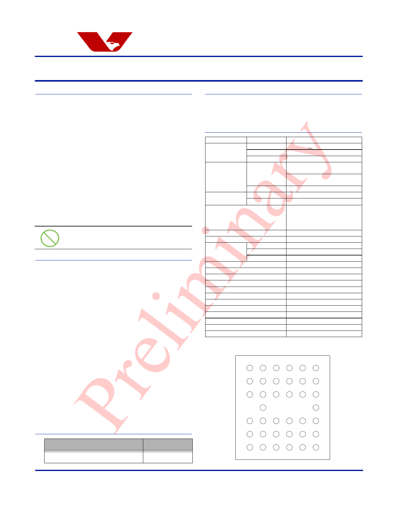
Figure 1 OV2640 Pin Diagram (Top View)
A1 A2 A3 A4 A5 A6
DOGND EXPST_B AGND SGND VREFN STROBE
B1 B2 B3 B4 B5 B6
DOVDD FREX AVDD SVDD SVDD PWDN
C1 C2 C3 C4 C5 C6
SIO_D SIO_C HREF XVCLK VREFH RESETB
D2 OV2640
VSYNC
D6
NC
E1 E2 E3 E4 E5 E6
Y1 Y0 PCLK EGND Y6 DGND
F1 F2 F3 F4 F5 F6
EVDD DVDD Y2 Y4 Y8 DVDD
G1 G2 G3 G4 G5 G6
EVDD DGND Y3 Y5 Y7 Y9
Version 1.6, February 28, 2006
Proprietary to OmniVision Technologies
1
1 page 
Omni ision
Functional Description
output, the OV2640 will output continuous live video data
unless in single frame transfer mode. Figure 18 and
Figure 19 show the detailed timing and Table 11 shows
the timing specifications for this mode.
Output Formatter
This block controls all output and data formatting required
prior to sending the image out.
Frame Rate Adjust
The OV2640 offers three methods for frame rate
adjustment:
• Clock prescaler: (see “CLKRC” on page 23)
By changing the system clock divide ratio and PLL,
the frame rate and pixel rate will change together.
This method can be used for dividing the frame/pixel
rate by: 1/2, 1/3, 1/4 … 1/64 of the input clock rate.
• Line adjustment: (see “REG2A” on page 26 and
“FRARL” on page 26)
By adding a dummy pixel timing in each line
(between HSYNC and pixel data out), the frame rate
can be changed while leaving the pixel rate as is.
• Vertical sync adjustment:
By adding dummy line periods to the vertical sync
period (see “ADDVSL” on page 26 and “ADDVSH”
on page 26 or see “FLL” on page 27 and “FLH” on
page 27), the frame rate can be altered while the
pixel rate remains the same.
Frame Rate Timing
Default frame timing is illustrated in Figure 15, Figure 16,
and Figure 17. Refer to Table 1 for the actual pixel rate at
different frame rates.
Table 1
Frame/Pixel Rates in UXGA Mode
Frame Rate (fps) 15 7.5 2.5 1.25
PCLK (MHz)
36 18
6
3
Digital Signal Processor (DSP)
Scaling Image Output
The OV2640 is capable of scaling down the image size
from CIF to 40x30. By using SCCB registers, the user can
output the desired image size. At certain image sizes,
HREF is not consistent in a frame.
Compression Engine
As shown in Figure 7, the Compression Engine consists
of three major blocks:
• DCT
• QZ
• Entropy Encoder
Figure 7 Compression Engine Block Diagram
Video Data
DCT
Compression Engine
QZ Entropy Encoder
Compressed
Stream
Scale Factor
Q-Table
H-Table Marker
Microcontroller
The OV2640 embeds an 8-bit microcontroller with
512-byte data memory and 4 KB program memory. It
provides the flexibility of decoding protocol commands
from the host for controlling the system, as well as the
ability to fine tune image quality.
This block controls the interpolation from Raw data to
RGB and some image quality control.
• Edge enhancement (a two-dimensional high pass
filter)
• Color space converter (can change Raw data to RGB
or YUV/YCbCr)
• RGB matrix to eliminate color cross talk
• Hue and saturation control
• Programmable gamma control
• Transfer 10-bit data to 8-bit
• White pixel canceling
• De-noise
SCCB Interface
The Serial Camera Control Bus (SCCB) interface controls
the CAMERACHIP operation. Refer to OmniVision
Technologies Serial Camera Control Bus (SCCB)
Specification for detailed usage of the serial control port.
Slave Operation Mode
The OV2640 can be programmed to operate in slave
mode (default is master mode).
When used as a slave device, COM7[3] (0x12), CLKRC[6]
(0x11), and COM2[2] (0x09) register bits should be set to
Version 1.6, February 28, 2006
Proprietary to OmniVision Technologies
5
5 Page 
Omni ision
Electrical Characteristics
Electrical Characteristics
Table 5
Absolute Maximum Ratings
Ambient Storage Temperature
-40ºC to +95ºC
VDD-A
Supply Voltages (with respect to Ground)
VDD-C
VDD-IO
All Input/Output Voltages (with respect to Ground)
Lead-free Temperature, Surface-mount process
4.5V
3V
4.5V
-0.3V to VDD-IO+1V
245ºC
ESD Rating, Human Body model
2000V
NOTE: Exceeding the Absolute Maximum ratings shown above invalidates all AC and DC electrical specifications and may
result in permanent device damage.
Table 6
DC Characteristics (-30°C < TA < 70°C)
Symbol
Parameter
Min Typ
Max
Supply
VDD-A
VDD-D
VDD-IO
IDDA-A
Supply voltage
Supply voltage
Supply voltagea
Active (Operating) Currentb
IDDA-D
Active (Operating) Currentb
IDDA-IO
Active (Operating) Currentb
IDDS-SCCB
IDDS-PWDN
Standby Currentb
Digital Inputs
2.5 2.8
3.0
1.14 1.2
1.26
1.71 2.8
3.3
30 40
25 (YUV)
35 (YUV)
35 (Compressed) 50 (Compressed)
6 10
12
600 1200
VIL Input voltage LOW
VIH Input voltage HIGH
CIN Input capacitor
Digital Outputs (standard loading 25 pF)
1.26
0.54
10
VOH Output voltage HIGH
VOL Output voltage LOW
Serial Interface Inputs
1.62
0.18
VIL SIO_C and SIO_D
-0.5 0
VIH SIO_C and SIO_D
1.26 1.8
a. 1.8V I/O is supported. Contact your local OmniVision FAE for further details.
b. VDD-A = 2.8V, VDD-D = 1.2V, and VDD-IO = 1.8V for 15 fps in UXGA mode
IDDS-SCCB refers to SCCB-initiated Standby, while IDDS-PWDN refers to PWDN pad-initiated Standby
0.54
2.3
Unit
V
V
V
mA
mA
mA
mA
µA
V
V
pF
V
V
V
V
Version 1.6, February 28, 2006
Proprietary to OmniVision Technologies
11
11 Page | ||
| Páginas | Total 30 Páginas | |
| PDF Descargar | [ Datasheet OV2640.PDF ] | |
Hoja de datos destacado
| Número de pieza | Descripción | Fabricantes |
| OV2640 | Color CMOS UXGA (2.0 MegaPixel) CAMERACHIP | OmniVision Technologies |
| Número de pieza | Descripción | Fabricantes |
| SLA6805M | High Voltage 3 phase Motor Driver IC. |
Sanken |
| SDC1742 | 12- and 14-Bit Hybrid Synchro / Resolver-to-Digital Converters. |
Analog Devices |
|
DataSheet.es es una pagina web que funciona como un repositorio de manuales o hoja de datos de muchos de los productos más populares, |
| DataSheet.es | 2020 | Privacy Policy | Contacto | Buscar |