|
|
PDF ICS527-02 Data sheet ( Hoja de datos )
| Número de pieza | ICS527-02 | |
| Descripción | Clock Slicer User Configurable PECL Input Zero Delay Buffer | |
| Fabricantes | Integrated Circuit Systems | |
| Logotipo |  |
|
Hay una vista previa y un enlace de descarga de ICS527-02 (archivo pdf) en la parte inferior de esta página. Total 8 Páginas | ||
|
No Preview Available !
www.DataSheet4U.com
ICS527-02
Clock Slicer User Configurable PECL Input Zero Delay Buffer
Description
The ICS527-02 Clock Slicer is the most flexible way to
generate a CMOS output clock from a PECL input
clock with zero skew. The user can easily configure the
device to produce nearly any output clock that is
multiplied or divided from the input clock. The part
supports non-integer multiplications and divisions. A
SYNC pulse indicates when the rising clock edges are
aligned with zero skew. Using Phase-Locked Loop
(PLL) techniques, the device accepts an input clock up
to 200 MHz and produces an output clock up to 160
MHz.
The ICS527-02 aligns rising edges on PECLIN with
FBIN at a ratio determined by the reference and
feedback dividers.
For a PECL input and output clock with zero delay, use
the ICS527-04.
For a CMOS input and PECL output with zero delay,
use the ICS527-03.
Features
• Packaged as 28-pin SSOP (150 mil body)
• Synchronizes fractional clocks rising edges
• PECL IN to CMOS OUT
• Pin selectable dividers
• Zero input to output skew
• User determines the output frequency—no software
needed
• Slices frequency or period
• Input clock frequency of 1.5 MHz to 200 MHz
• Output clock frequencies from 2.5 MHz to 160 MHz
• Very low jitter
• Duty cycle of 45/55
• Operating voltage of 3.3 V
• Advanced, low-power CMOS process
• Industrial temperature version available
Block Diagram
PECLIN
PECLIN
R6:R0
7
Reference
Divider
FBIN
Feedback
Divider
7
F6:F0
2 VDD
Phase Comparator,
Charge Pump, and
Loop Filter
VCO
SYNC
2 GND
PDTS
Output
Divider
2
S1:S0
33 ohm
CLK1
Divide
by 2
1
0
DIV2
33 ohm
CLK2
Feedback can
come from
CLK1 or CLK2
(not both)
www.DataSheet4U.com
MDS 527-02 F
1
Revision 022806
Integrated Circuit Systems, Inc. ● 525 Race Street, San Jose, CA 95126 ● tel (408) 297-1201 ● www.icst.com
1 page 
www.DataSheet4U.com
ICS527-02
Clock Slicer User Configurable PECL Input Zero Delay Buffer
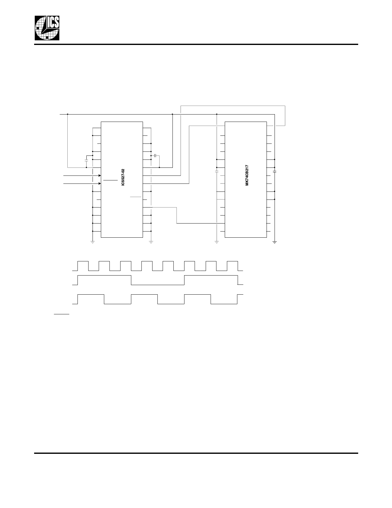
Multiple Output Example
In this example, an input clock of 125 MHz is used. Eight copies of 50 MHz are required as are eight copies
of 25 MHz, de-skewed and aligned to the 125 MHz input clock. The following solution uses the
MK74CB217 which has dual 1 to 8 buffers with low pin-to-pin skew.
VDD
0.01µF
125 MHz
125 MHz
R5
R6
DIV2
S0
S1
VDD
PECLIN
PECLIN
GND
OECLK2
F0
F1
F2
F3
R4
R3
R2
R1
R0
VDD
CLK1
CLK2
GND
PDTS
FBIN
F6
F5
F4
0.01µF
50M
25M
0.01µF
INA
QA0
QA1
QA2
VDD
VDD
QA3
QA4
GND
GND
QA5
QA6
QA7
OEA
INB
QB0
QB1
QB2
VDD
VDD
QB3
QB4
GND
GND
QB5
QB6
QB7
OEB
0.01µF
The layout design above produces the waveforms shown below. Note: Series terminating resistors are not shown.
125 MHz,
PECLIN
25 MHz,
QA0-7
50 MHz,
QB0-7
PECLIN not shown
PCB Layout Recommendations
For optimum device performance and lowest output
phase noise, the following guidelines should be
observed.
1) Each 0.01µF decoupling capacitor should be
mounted on the component side of the board as close
to the VDD pin as possible. No via’s should be used
between decoupling capacitor and VDD pin. The PCB
trace to VDD pin should be kept as short as possible,
as should the PCB trace to the ground via.
2) To minimize EMI the 33Ω series termination resistor,
if needed, should be placed close to the clock outputs.
3) An optimum layout is one with all components on the
same side of the board, minimizing vias through other
signal layers. Other signal traces should be routed
away from the ICS527-02. This includes signal traces
just underneath the device, or on layers adjacent to the
ground plane layer used by the device.
www.DataSheet4U.com
MDS 527-02 F
5
Revision 022806
Integrated Circuit Systems, Inc. ● 525 Race Street, San Jose, CA 95126 ● tel (408) 297-1201 ● www.icst.com
5 Page | ||
| Páginas | Total 8 Páginas | |
| PDF Descargar | [ Datasheet ICS527-02.PDF ] | |
Hoja de datos destacado
| Número de pieza | Descripción | Fabricantes |
| ICS527-01 | User Configurable Zero Delay Buffer | Integrated Circuit Systems |
| ICS527-02 | Clock Slicer User Configurable PECL Input Zero Delay Buffer | Integrated Circuit Systems |
| ICS527-03 | Clock Slicer User Configurable PECL Output Zero Delay Buffer | Integrated Circuit Systems |
| ICS527-04 | Clock Slicer User Configurable PECL input Zero Delay Buffer | Integrated Circuit Systems |
| Número de pieza | Descripción | Fabricantes |
| SLA6805M | High Voltage 3 phase Motor Driver IC. |
Sanken |
| SDC1742 | 12- and 14-Bit Hybrid Synchro / Resolver-to-Digital Converters. |
Analog Devices |
|
DataSheet.es es una pagina web que funciona como un repositorio de manuales o hoja de datos de muchos de los productos más populares, |
| DataSheet.es | 2020 | Privacy Policy | Contacto | Buscar |
