|
|
|
PDF PC8374L Data sheet ( Hoja de datos )
| Número de pieza | PC8374L | |
| Descripción | SensorPathTM SuperI/O with Glue Functions | |
| Fabricantes | National Semiconductor | |
| Logotipo | ||
Hay una vista previa y un enlace de descarga de PC8374L (archivo pdf) en la parte inferior de esta página. Total 70 Páginas | ||
|
No Preview Available !
www.DataSheet4U.com Winbond Electronics Corp. Advanced PC Product Center
Preliminary
May 2004
Revision 1.1
PC8374L
SensorPathTM SuperI/O with Glue Functions
General Description
The National Semiconductor PC8374L Advanced I/O prod-
uct is a member of the PC837x SuperI/O family. All PC837x
devices are highly integrated and are pin and software com-
patible, thus providing drop-in interchangeability and
enabling a variety of assembly options using only a single
motherboard and BIOS.
PC8374L integration allows for a smaller system board size and
saves on total system cost.
The PC8374L includes legacy SuperI/O functions, system
glue functions, health monitoring and control, commonly
used functions such as GPIO, and ACPI-compliant Power
Management support.
The PC8374L integrates miscellaneous analog and digital
system glue functions to reduce the number of discrete
components required. The host communicates with the
functions integrated in the PC8374L device through an LPC
Bus Interface.
The PC8374L extended wake-up support complements the
ACPI controller in the chipset. The System Wake-Up Control
(SWC) module, powered by VSB3, supports a flexible wake-
up mechanism.
The PC8374L supports both I/O and memory mapping of
module registers and enables building legacy-free systems.
Outstanding Features
■ SensorPath interface to LMxx sensor devices for system
health support
■ Fan monitor and control
■ Heceta6-compatible register set, accessible via the LPC
interface and SMBus
■ Glue functions to complement the South Bridge func-
tionality
■ VSB3-powered Power Management with 19 wake-up
sources
■ Controls three LED indicators
■ 16 GPIO ports with a variety of wake-up options
■ I/O-mapped and memory-mapped registers
■ Legacy modules: Parallel Port, Floppy Disk Controller
(FDC), two Serial Ports, Slow InfraRed Port and a Key-
board and Mouse Controller (KBC)
■ LPC interface, based on Intel’s LPC Interface Specifica-
tion Revision 1.1, August 2002
■ PC01 Revision 1.0 and Advanced Configuration and
Power Interface (ACPI) Specification Revision 2.0 compliant
■ 128-pin PQFP package
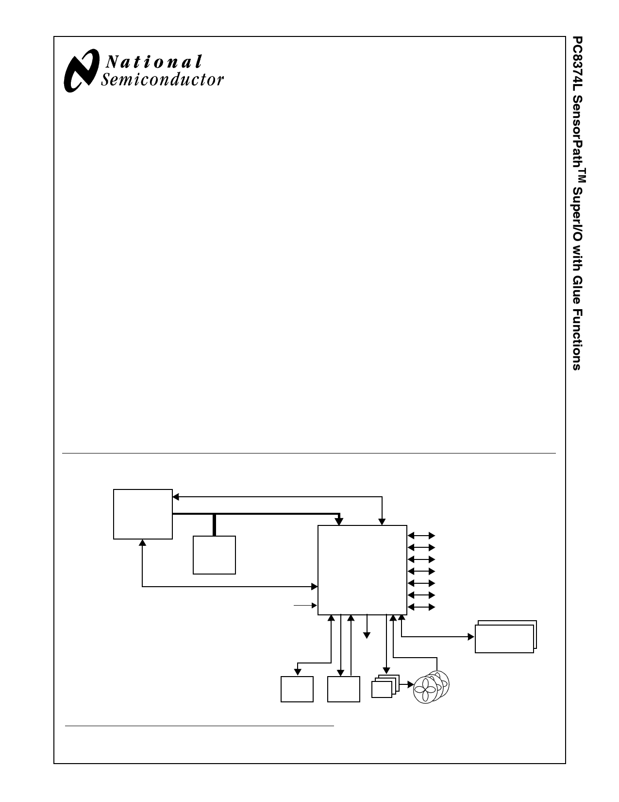
Block Diagram
South Bridge
LPC Bus
System
BIOS
SMBus I/F
VBAT
Power Management
PC8374L
Serial Interfaces
Parallel Port Interfaces
Floppy Drive Interface
PS/2 Interfaces
KBC Ports
Infrared Interface
GPIO Ports
www.DataSheet4U.com
Reset
Logic
LEDs
SensorPathTM I/F
Tacho
LMxx Sensors
Power
Supply
PWM
DDrDvrvrv
National Semiconductor and TRI-STATE are registered trademarks of National Semiconductor Corporation.
SensorPath is a trademark of National Semiconductor Corporation.
All other brand or product names are trademarks or registered trademarks of their respective holders.
© 2004 National Semiconductor Corporation
www.national.com
1 page 
www.DataSheet4U.com Winbond Electronics Corp. Advanced PC Product Center
Revision Record (Continued)
Revision Date
August 12, 2003
October 13, 2003
November 20, 2003
February 3, 2004
May 2004
Status
Draft Revision 0.7
Draft Revision 0.8
Preliminary Revision 0.9
Preliminary Revision 1.0
Preliminary Revision 1.1
Comments
Change PWRGD_3V functionality
Add details to SERIAL PORT 2 (SP2) WITH INFRARED Section
Change in HMSMBCF register
Typos and clarifications
Health Management: Added support for more LMxx devices - see
overview Section 9.2.2 - added a table of temp channel
association. New HM registers: Status Register 3-4, Monitoring
Control, Extended FANPWM Control 1-2, Tachometer Monitoring
Control, Channels Vdd configuration, Temp Critical Limit Zone1-
3,Temp Zone1-3 Gain and Offset Correction. New HM LPC
registers:HMINT_STS3, HMINT_EN#, HMSENS_STS3,
HMS_EN1-3, SMI/SCI_ROUT. Functional description updated.
Temp Reading registers updated.
Maximum PWM duty cycle,
Fans setting time to the maximum duty cycle,
Changed default mode of LED control
Correct Table 3 on page 18
Rename LMxx sensor device
Removed FPRST
Changed reset value of FANTACH registers to FF
Changed reset value of FANOFF to 1
Added Package Thermal Information
Typos and clarifications
● Changes to the Health Management Chapter
● Device Characteristics: Minimum value of tCH, tCL reduced to
20 ns
● Typos and Clarifications
● Added LM sensor devices
● Changed VBAT external capacitor requirement to 1 µF
● Typos and Clarifications
● Glue Functions: Removed 2.5V voltage divider circuit for SM-
Bus Voltage Translation system diagram
● Typos and Clarifications
www.DataSheet4U.com
Revision 1.1
5
www.national.com
5 Page 
www.DataSheet4U.com Winbond Electronics Corp. Advanced PC Product Center
Table of Contents (Continued)
9.2.2 Parallel Port Register Map ......................................................................................... 194
9.2.3 Parallel Port Bitmap Summary .................................................................................. 195
9.3 SERIAL PORT 1 (SP1) ............................................................................................................ 196
9.3.1 General Description ................................................................................................... 196
9.3.2 Register Bank Overview ............................................................................................ 196
9.3.3 SP1 Register Maps .................................................................................................... 197
9.3.4 SP1 Bitmap Summary ............................................................................................... 199
9.4 SERIAL PORT 2 (SP2) ............................................................................................................ 200
9.4.1 General Description ................................................................................................... 200
9.4.2 Register Bank Overview ............................................................................................ 200
9.4.3 SP2 Register Map ..................................................................................................... 202
9.4.4 SP2 Bitmap Summary ............................................................................................... 204
9.5 SERIAL PORT 2 (SP2) WITH INFRARED .............................................................................. 206
9.5.1 General Description ................................................................................................... 206
9.5.2 UART Register Bank Overview ................................................................................. 206
9.5.3 SP2 Register Map ..................................................................................................... 207
9.6 KEYBOARD AND MOUSE CONTROLLER (KBC) ................................................................. 210
9.6.1 General Description ................................................................................................... 210
9.6.2 KBC Register Map ..................................................................................................... 211
9.6.3 KBC Bitmap Summary ............................................................................................... 211
10.0 Device Characteristics
10.1 GENERAL DC ELECTRICAL CHARACTERISTICS ............................................................... 212
10.1.1 Recommended Operating Conditions ....................................................................... 212
10.1.2 Absolute Maximum Ratings ....................................................................................... 212
10.1.3 Capacitance .............................................................................................................. 212
10.1.4 Power Consumption under Recommended Operating Conditions ............................ 213
10.1.5 Voltage Thresholds .................................................................................................... 213
10.2 DC CHARACTERISTICS OF PINS, BY I/O BUFFER TYPES ................................................ 213
10.2.1 Input, TTL Compatible ............................................................................................... 213
10.2.2 Input, TTL Compatible, with Schmitt Trigger ............................................................. 214
10.2.3 Input, TTL Compatible, with 200 mV Schmitt Trigger ................................................ 214
10.2.4 Input, TTL Compatible, with 400 mV Schmitt Trigger ................................................ 214
10.2.5 Input, PCI 3.3V Compatible ....................................................................................... 215
10.2.6 Input, SMBus Compatible .......................................................................................... 215
10.2.7 Analog Input .............................................................................................................. 215
10.2.8 Output, TTL/CMOS Compatible, Push-Pull Buffer .................................................... 215
10.2.9 Output, TTL/CMOS Compatible, Open-Drain Buffer ................................................. 216
10.2.10 Output, PCI 3.3V Compatible .................................................................................... 216
10.2.11 Analog Output ............................................................................................................ 216
10.2.12 Input/Output Switch, SMBus Compatible .................................................................. 216
10.2.13 Exceptions ................................................................................................................. 217
www.DataS1h0e.2e.1t44UT.ecromminology ............................................................................................................... 217
10.3 INTERNAL RESISTORS ......................................................................................................... 218
10.3.1 Pull-Up Resistor ......................................................................................................... 218
10.3.2 Pull-Down Resistor .................................................................................................... 218
Revision 1.1
11 www.national.com
11 Page | ||
| Páginas | Total 70 Páginas | |
| PDF Descargar | [ Datasheet PC8374L.PDF ] | |
Hoja de datos destacado
| Número de pieza | Descripción | Fabricantes |
| PC8374L | SensorPathTM SuperI/O with Glue Functions | National Semiconductor |
| PC8374T | SafeKeeper Desktop Trustedl/O | National Semiconductor |
| PC8374T | SafeKeeper Desktop Trustedl/O | National Semiconductor |
| Número de pieza | Descripción | Fabricantes |
| SLA6805M | High Voltage 3 phase Motor Driver IC. |
Sanken |
| SDC1742 | 12- and 14-Bit Hybrid Synchro / Resolver-to-Digital Converters. |
Analog Devices |
|
DataSheet.es es una pagina web que funciona como un repositorio de manuales o hoja de datos de muchos de los productos más populares, |
| DataSheet.es | 2020 | Privacy Policy | Contacto | Buscar |