|
|
PDF LC876796B Data sheet ( Hoja de datos )
| Número de pieza | LC876796B | |
| Descripción | (LC876772B/80B86B) 8_bit Signal Chup Microcontroller | |
| Fabricantes | Sanyo Electric | |
| Logotipo |  |
|
Hay una vista previa y un enlace de descarga de LC876796B (archivo pdf) en la parte inferior de esta página. Total 26 Páginas | ||
|
No Preview Available !
( DataSheet : www.DataSheet4U.com )
CMOS IC
LC876796B/80B/72B
8-Bit Single Chip Microcontroller
LC876796B
8 bit Single Chip Microcontroller incorporating 96KB ROM and 2048 byte RAM on chip
LC876780B
8 bit Single Chip Microcontroller incorporating 80KB ROM and 2048 byte RAM on chip
LC876772B
8 bit Single Chip Microcontroller incorporating 72KB ROM and 2048 byte RAM on chip
Overview
The LC876796B/ LC876780B/ LC876772B are 8 bit single chip microcomputers with the following on-chip
functional blocks:
- CPU: operable at a minimum bus cycle time of 100ns
- On-chip ROM Maximum Capacity : LC876796B 96K bytes
LC876780B 80K bytes
LC876772B 72K bytes
- On-chip RAM: 2048 bytes
- VFD automatic display controller / driver
- 16 bit timer / counter (can be divided into two 8 bit timers)
- 16 bit timer / counter (can be divided into two 8 bit timers / two 8 bit PWM)
- four 8 bit timer with prescaler
- timer for use as date / time clock
- High speed clock counter
- System clock divider function
- synchronous serial I/O port (with automatic block transmit / receive function)
- asynchronous / synchronous serial I/O port
- 14-channel × 8-bit AD converter
- Weak signal detector
- 21-source 10-vectored interrupt system
All of the above functions are fabricated on a single chip.
Ver:1.06
M2003
www.DataSheet4U.com
May 20, 2003 SYSTEM-BIZ Div. S.Kubota 1/26
1 page 
LC876796B/80B/72B
-HOLD mode
HOLD mode is used to reduce power consumption. Both program execution and peripheral
circuits are stopped.
1) CF, RC and crystal oscillation circuits stop automatically.
2) Release occurs on any of the following conditions.
(1) input to the reset pin goes low
(2) a specified level is input at least one of INT0, INT1, INT2, INT4, INT5
(3) an interrupt condition arises at port 0
-X’tal HOLD made
X’tal HOLD mode is used to reduce power consumption. Program execution is stopped.
All peripheral circuits except the base timer are stopped.
1) CF and RC oscillation circuits stop automatically.
2) Crystal oscillator is maintained in its state at HOLD mode inception.
3) Release occurs on any an any of the following conditions
(1) input to the reset pin goes low
(2) a specified level is input to at least one of INT0, INT1, INT2, INT4, INT5
(3) an interrupt condition arises at port 0
(4) an interrupt condition arises at the base-timer
(20) Factory shipment
-delivery form QIP100E (LEAD FREE PRODUCT)
(21) Development tools
- Evaluation chip : LC876093
- Emulator
: EVA62S + ECB876600 (Evaluation chip board) + SUB876700 + POD100QFP
: ICE-B877300 + SUB876700 + POD100QFP
- Flash ROM version: LC87F67C8A
5 Page 
LC876796B/80B/72B
Port Output Configuration
Output configuration and pull-up/pull-down resistor options are shown in the following table.
Input/output is possible even when port is set to output mode.
Terminal
Option applies to: Options
Output Format
Pull-up resistor Pull-down resistor
P00 to P07
1 bit units
1
2
CMOS
15V Nch-open drain
Programmable
(Note 1)
None
-
-
P10 to P17
each bit
1
CMOS
Programmable
-
2
Nch-open drain
Programmable
-
P30 to P37
each bit
1
CMOS
Programmable
-
2 15V Nch-open drain
None
-
P70
-
None
Nch-open drain
Programmable
-
P71 to P73
- None
CMOS
Programmable
-
P80 to P87
- None Nch-open drain
None
-
S0/T0 to S15/T15
S16 to S51
XT1
-
None High voltage Pch-open drain
-
- None
Input only
None
None
-
XT2
-
Output for 32.768kHz crystal
None
None oscillation
Note 1: Programmable pull-up resisters of Port 0 can be attached in nibble units (P00-03, P04-07).
-
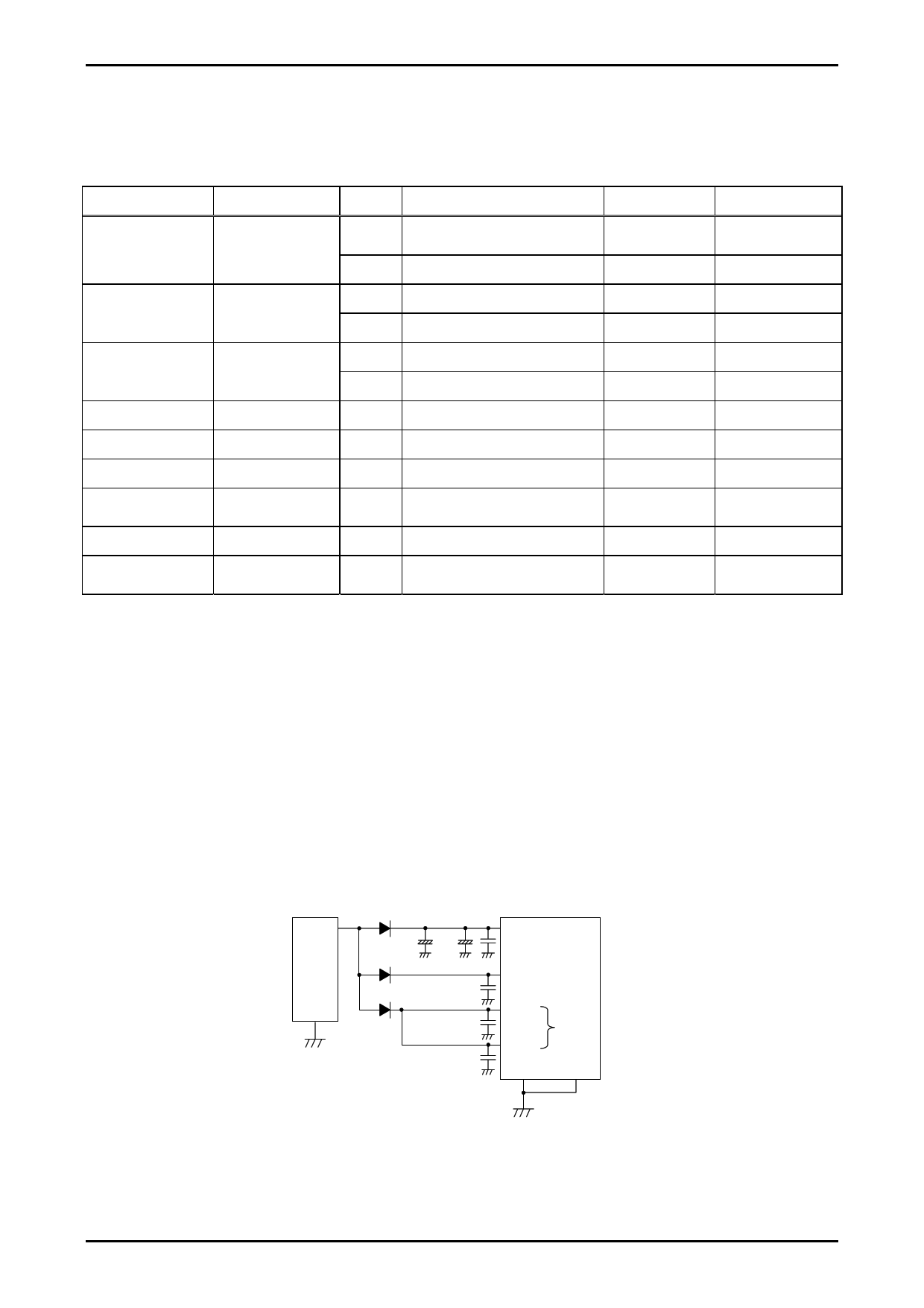
* Note 1: Connect as follows to reduce noise on VDD and increase the back-up time.
VSS1, and VSS2 must be connected together and grounded.
* Note 2: The power supply for the internal memory is VDD1 but it uses the VDD2 as the power supply for
ports. When the VDD2 is not backed up, the port level does not become “H” even if the port latch is
in the “H” level. Therefore, when the VDD2 is not backed up and the port latch is “H” level, the port
level is unstable in the HOLD mode, and the back up time becomes shorter because the through
current runs from VDD to GND in the input buffer.
If VDD2 is not backed up, output “L” by the program or pull the port to “L” by the external circuit
in the HOLD mode so that the port level becomes “L” level and unnecessary current consumption is
prevented.
Power
Supply
LSI
VDD1
Back-up capacitors
VDD2
VDD3
VDD4
VFD
Powers
VSS1 VSS2
11 Page | ||
| Páginas | Total 26 Páginas | |
| PDF Descargar | [ Datasheet LC876796B.PDF ] | |
Hoja de datos destacado
| Número de pieza | Descripción | Fabricantes |
| LC876796B | (LC876772B/80B86B) 8_bit Signal Chup Microcontroller | Sanyo Electric |
| Número de pieza | Descripción | Fabricantes |
| SLA6805M | High Voltage 3 phase Motor Driver IC. |
Sanken |
| SDC1742 | 12- and 14-Bit Hybrid Synchro / Resolver-to-Digital Converters. |
Analog Devices |
|
DataSheet.es es una pagina web que funciona como un repositorio de manuales o hoja de datos de muchos de los productos más populares, |
| DataSheet.es | 2020 | Privacy Policy | Contacto | Buscar |
