|
|
|
PDF ICX039DLA Data sheet ( Hoja de datos )
| Número de pieza | ICX039DLA | |
| Descripción | Diagonal 8mm (Type 1/2) CCD Image Sensor for CCIR Black-and-White Video Cameras | |
| Fabricantes | Sony Corporation | |
| Logotipo | ||
Hay una vista previa y un enlace de descarga de ICX039DLA (archivo pdf) en la parte inferior de esta página. Total 20 Páginas | ||
|
No Preview Available !
ICX039DLA
Diagonal 8mm (Type 1/2) CCD Image Sensor for CCIR Black-and-White Video Cameras
Description
The ICX039DLA is an interline CCD solid-state
image sensor suitable for CCIR black-and-white
video cameras with a diagonal 8mm (Type 1/2)
system. Smear, sensitivity, D-range, S/N and other
characteristics have been greatly improved
compared with the ICX039BLA. High sensitivity and
low dark current are achieved through the adoption
of HAD (Hole-Accumulation Diode) sensors.
This chip features a field period readout system and
an electronic shutter with variable charge-storage
time.
This chip is compatible with and can replace the
ICX039BLA.
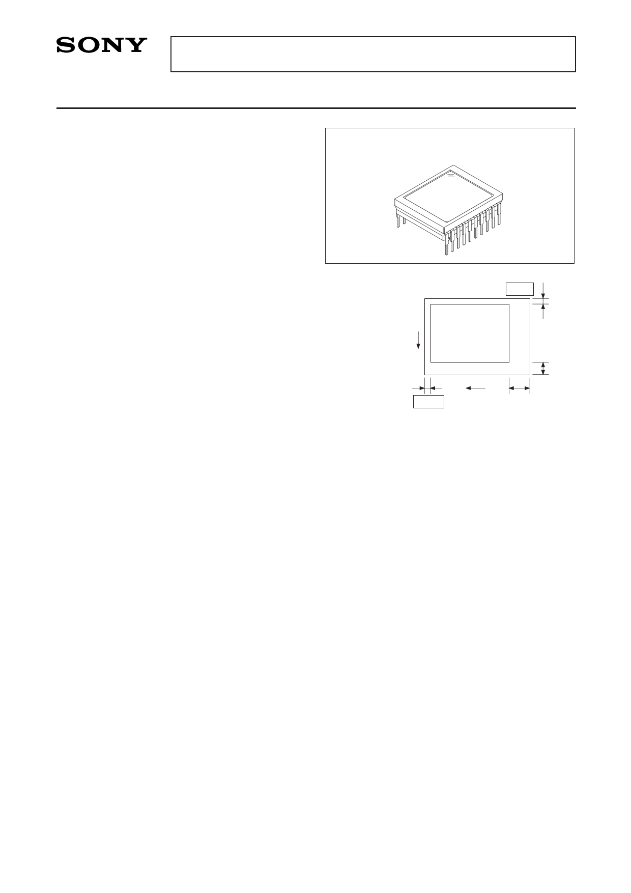
20 pin DIP (Cer-DIP)
Pin 1
2
V
Features
• Low smear (–20dB compared with the ICX039BLA)
• High sensitivity (+3.0dB compared with the ICX039BLA)
3
H 40
Pin 11
• High D range (+2.5dB compared with the ICX039BLA)
• High S/N
• High resolution and low dark current
Optical black position
(Top View)
• Excellent antiblooming characteristics
• Continuous variable-speed shutter
• Substrate bias:
Adjustment free (external adjustment also possible with 6 to 14V)
• Reset gate pulse: 5Vp-p adjustment free (drive also possible with 0 to 9V)
• Horizontal register: 5V drive
12
Device Structure
• Interline CCD image sensor
• Image size:
Diagonal 8mm (Type 1/2)
• Number of effective pixels: 752 (H) x 582 (V) approx. 440K pixels
• Total number of pixels: 795 (H) x 596 (V) approx. 470K pixels
• Chip size:
7.95mm (H) x 6.45mm (V)
• Unit cell size:
8.6µm (H) x 8.3µm (V)
• Optical black:
Horizontal (H) direction : Front 3 pixels, rear 40 pixels
Vertical (V) direction : Front 12 pixels, rear 2 pixels
• Number of dummy bits: Horizontal 22
Vertical 1 (even fields only)
• Substrate material:
Silicon
Sony reserves the right to change products and specifications without prior notice. This information does not convey any license by
any implication or otherwise under any patents or other right. Application circuits shown, if any, are typical examples illustrating the
operation of the devices. Sony cannot assume responsibility for any problems arising out of the use of these circuits.
–1–
E95714C99
1 page 
ICX039DLA
Clock Voltage Conditions
Item Symbol
Readout clock voltage VVT
VVH1, VVH2
VVH3, VVH4
VVL1, VVL2,
VVL3, VVL4
VφV
Vertical transfer clock
voltage
| VVH1 – VVH2 |
VVH3 – VVH
VVH4 – VVH
VVHH
VVHL
VVLH
VVLL
Horizontal transfer
clock voltage
VφH
VHL
Reset gate clock
voltage∗1
VRGL
VφRG
VRGLH – VRGLL
Substrate clock voltage VφSUB
Min.
Typ.
Max.
Unit
Waveform
diagram
Remarks
14.55 15.0 15.45 V
1
–0.05 0 0.05 V
2 VVH = (VVH1 + VVH2)/2
–0.2 0 0.05 V
2
–9.6 –9.0 –8.5 V
2 VVL = (VVL3 + VVL4)/2
8.3 9.0 9.65 Vp-p
0.1 V
–0.25
0.1 V
–0.25
0.1 V
0.5 V
0.5 V
0.5 V
0.5 V
4.75 5.0 5.25 Vp-p
–0.05 0 0.05 V
∗1 V
4.5 5.0 5.5 Vp-p
0.8 V
23.0 24.0 25.0 Vp-p
2
2
2
2
2
2
2
2
3
3
4
4
4
5
VφV = VVHn – VVLn (n = 1 to 4)
High-level coupling
High-level coupling
Low-level coupling
Low-level coupling
Low-level coupling
∗1 Input the reset gate clock without applying a DC bias. In addition, the reset gate clock can also be driven
with the following specifications.
Item
Reset gate clock
voltage
Symbol
VRGL
VφRG
Min.
Typ.
Max.
Unit
Waveform
diagram
–0.2 0 0.2 V
4
8.5 9.0 9.5 Vp-p
4
Remarks
–5–
5 Page 
ICX039DLA
Image Sensor Characteristics Measurement Method
Measurement conditions
1) In the following measurements, the device drive conditions are at the typical values of the bias and clock
voltage conditions. (When used with substrate bias external adjustment, set the substrate voltage to the
value indicated on the device.)
2) In the following measurements, spot blemishes are excluded and, unless otherwise specified, the optical
black (OB) level is used as the reference for the signal output, and the value measured at point [∗A] in the
drive circuit example is used.
Definition of standard imaging conditions
1) Standard imaging condition I:
Use a pattern box (luminance: 706cd/m2, color temperature of 3200K halogen source) as a subject.
(Pattern for evaluation is not applicable.) Use a testing standard lens with CM500S (t = 1.0mm) as an IR cut
filter and image at F8. The luminous intensity to the sensor receiving surface at this point is defined as the
standard sensitivity testing luminous intensity.
2) Standard imaging condition II:
Image a light source (color temperature of 3200K) with a uniformity of brightness within 2% at all angles.
Use a testing standard lens with CM500S (t = 1.0mm) as an IR cut filter. The luminous intensity is adjusted
to the value indicated in each testing item by the lens diaphragm.
1. Sensitivity
Set to standard imaging condition I. After selecting the electronic shutter mode with a shutter speed of
1/250s, measure the signal output (Vs) at the center of the screen and substitute the value into the
following formula.
S = Vs x
250
50
[mV]
2. Saturation signal
Set to standard imaging condition II. After adjusting the luminous intensity to 10 times the intensity with the
average value of the signal output, 200mV, measure the minimum value of the signal output.
3. Smear
Set to standard imaging condition II. With the lens diaphragm at F5.6 to F8, adjust the luminous intensity to
500 times the intensity with the average value of the signal output, 200mV. When the readout clock is
stopped and the charge drain is executed by the electronic shutter at the respective H blankings, measure
the maximum value (VSm [mV]) of the signal output and substitute the value into the following formula.
Sm =
VSm
200
x
1
500
x
1
10
x 100 [%] (1/10V method conversion value)
4. Video signal shading
Set to standard imaging condition II. With the lens diaphragm at F5.6 to F8, adjust the luminous intensity so
that the average value of the signal output is 200mV. Then measure the maximum (Vmax [mV]) and
minimum (Vmin [mV]) values of the signal output and substitute the values into the following formula.
SH = (Vmax – Vmin)/200 x 100 [%]
– 11 –
11 Page | ||
| Páginas | Total 20 Páginas | |
| PDF Descargar | [ Datasheet ICX039DLA.PDF ] | |
Hoja de datos destacado
| Número de pieza | Descripción | Fabricantes |
| ICX039DLA | Diagonal 8mm (Type 1/2) CCD Image Sensor for CCIR Black-and-White Video Cameras | Sony Corporation |
| ICX039DLB | Diagonal 8mm (Type 1/2) CCD Image Sensor for CCIR Black-and-White Video Cameras | Sony Corporation |
| Número de pieza | Descripción | Fabricantes |
| SLA6805M | High Voltage 3 phase Motor Driver IC. |
Sanken |
| SDC1742 | 12- and 14-Bit Hybrid Synchro / Resolver-to-Digital Converters. |
Analog Devices |
|
DataSheet.es es una pagina web que funciona como un repositorio de manuales o hoja de datos de muchos de los productos más populares, |
| DataSheet.es | 2020 | Privacy Policy | Contacto | Buscar |