|
|
|
PDF HPL5331 Data sheet ( Hoja de datos )
| Número de pieza | HPL5331 | |
| Descripción | 3A Bus Termination Regulator | |
| Fabricantes | HiPAC | |
| Logotipo | ||
Hay una vista previa y un enlace de descarga de HPL5331 (archivo pdf) en la parte inferior de esta página. Total 20 Páginas | ||
|
No Preview Available !
HPL5331
3A Bus Termination Regulator
Features
General Description (Cont.)
• Provide Bi-direction Current
- Sourcing or Sinking Current up to 3A
• 1.25V/0.9V Output for DDR I/II Applications
• Fast Transient Response
• High Output Accuracy
- ±20mV over Load, VOUT Offset and
Temperature
• Adjustable Output Voltage by External Resistors
• Current-Limit Protection
• On-Chip Thermal Shutdown
• Shutdown for Standby or Suspend Mode
On-chip thermal shutdown provides protection against
any combination of overload that would create ex-
cessive junction temperature. The output voltage of
HPL5331 track the voltage at VREF pin. A resistor
divider connected to VIN, GND and VREF pins is
used to provide a half voltage of VIN to VREF pin. In
addition, an external ceramic capacitor and an open-
drain transistor connected to VREF pin provides soft-
start and shutdown control respectively. Pulling and
holding the VREF to GND shuts off the output. The
output of HPL5331 will be high impedance after being
shut down by VREF or thermal shutdown function.
• Simple SOP-8, SOP-8-P with thermal pad,
TO-252- 5 and TO-263-5 Packages
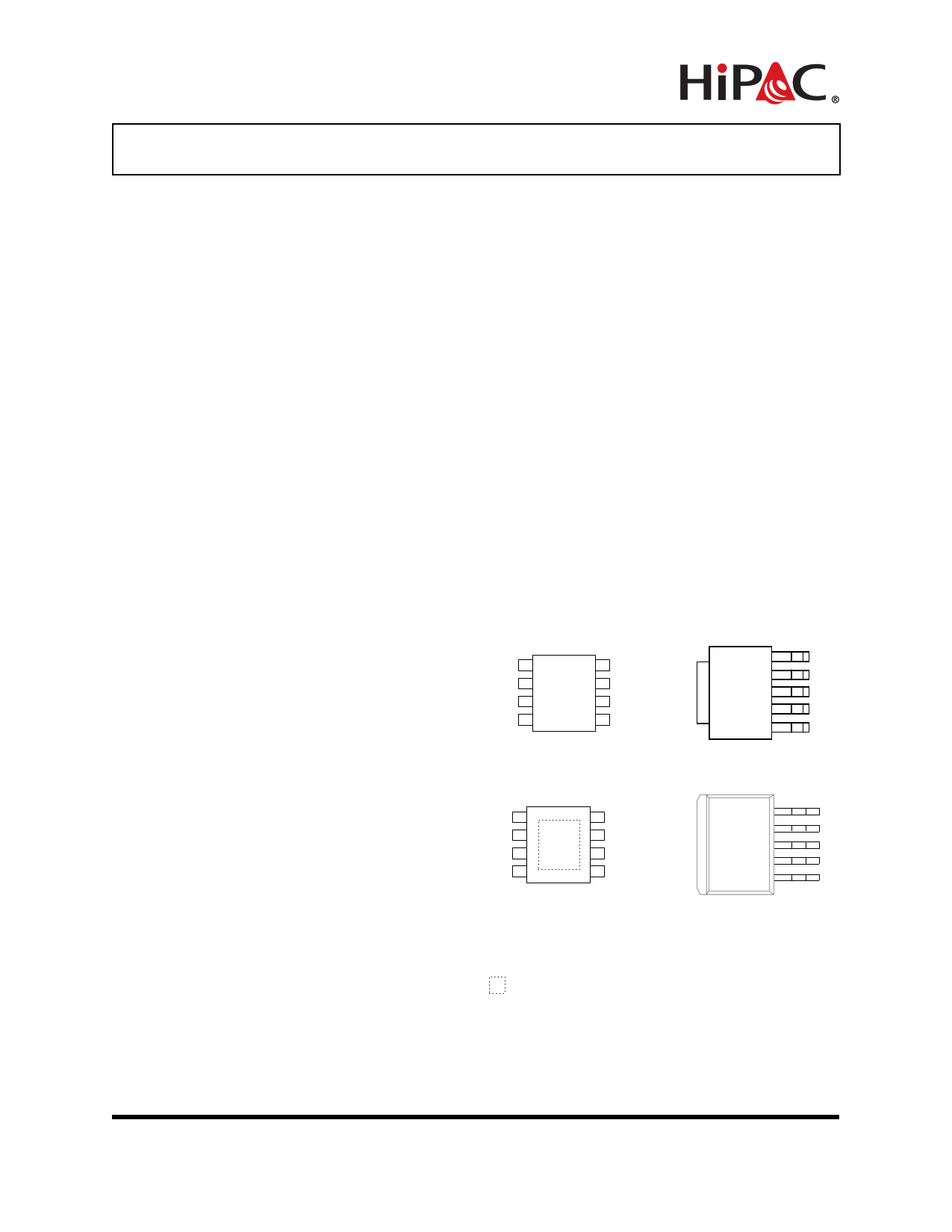
Pin Configuration
Applications
• DDR I/II SDRAM Termination
• SSTL-2/3 Termination Voltage
• Applications Requiring the Regulator with
Bi-direction 3A Current Capability
General Description
The HPL5331 linear regulator is designed to provide a
regulated voltage with bi-directional output current for
DDR-SDRAM termination. The HPL5331 integrates
two power transistors to source or sink current up to
3A. It also incorporate current-limit, thermal shutdown
and shutdown control functions into a single chip. Cur-
rent-limit circuit limits the short-circuit current.
VIN
GND
VREF
VOUT
1
2
3
4
8 VCNTL
7 VCNTL
TAB is VCNTL
6 VCNTL
5 VCNTL
VOUT
VREF
VCNTL
GND
VIN
SOP-8 (Top View)
TO-252-5 (Top View)
VIN
GND
VREF
VOUT
1
2
3
4
8 NC
7 NC
TAB is VCNTL
6 VCNTL
5 NC
5 VOUT
4 VREF
3 VCNTL
2 GND
1 VIN
SOP-8-P (Top View) TO-263-5 (Top View)
NC = No internal connection
= Thermal Pad
(connected to GND plane for better heat
dissipation)
Copyright HIPAC Semiconductor, Inc.
Rev. A.8 - Oct., 2003
1
www.hipacsemi.com
1 page 
HPL5331
Typical Application Circuit
1. VOUT=1.25V/0.9V Application
VCN TL
+3 .3 V
VIN
+2 .5 V/1 .8 V
C IN
470uF
Shu td o w n
GND
Q1
R1
1k
R2
1k
VIN VC N TL
VREF GND VOUT
VR EF
C SS
0 .1 u F
C CN TL
47uF
COUT : 470µF, ESR=25mΩ
R1, R2 : 1kΩ, 1%
Q1 : HPM2300 AC
Note : Since R1 and R2 are very small, the voltage offset
caused by the bias current of VREF can be ignore.
2. VOUT=1.4V Application
VCNT L
+5V
VIN
+2.8V
C IN
470µF
GND
VIN VC N TL
R1
1k VR EF GN D VOU T
VRE F
R2 CSS
1k 0.1µF
CCNT L
47µF
VOU T
+1 .2 5 V/0.9 V
-3~+3A
C OUT
470uF
GND
VO U T
+ 1.4V/
-3~ +3 A
C O UT
470µF
GND
Copyright HIPAC Semiconductor, Inc.
Rev. A.8 - Oct., 2003
5
www.hipacsemi.com
5 Page 
HPL5331
Application Information
Power Inputs
Input power sequence are not required for VIN and
VCNTL. However, do not apply a voltage to VOUT
when there is not voltage VCNTL. This is due to the
internal parasitic diodes between VOUT to VIN and
VOUT to VCNTL which will be forward bias. The
HPL5331 can source few current or sinks current up
to 3A for load when the input Voltage at VIN is not
present.
Reference Voltage
A reference voltage is applied at the VREF pin by a
resistor divider between VIN and GND pins. Normally
the bias current of the VREF pin flows out of the IC
and is about 150nA(typ.), creating voltage offset at
the resistor divider and affecting the output voltage
accuracy. The recommended resistor is <5kΩ to
maintain the accuracy of the output voltage. An ex-
ternal bypass capacitor is also connected to VREF.
The capacitor and the resistor divider form a low-
pass filter to reduce the inherent reference noise from
VIN. A ceramic capacitor can be use and is selected
to be greater than 0.1µF. Connected the capacitor
as close to VREF as possible for optimal effect. More
capacitance and large resistor divider will increase
the soft-start interval. Do not place any additional load-
ing on this reference input pin.
Output Capacitor
The HPL5331 requires a proper output capacitor to
maintain stability over full temperature and current
ranges, and improve transient response. The output
capacitor selection is dependent upon the ESR
(equivalent series resistance) and capacitance of the
output capacitor over full temperature range. The fol-
lowing chart shows the stable region of the output
capacitor for HPL5331. The stable region is above the
curve, indicating minimum required ESR and capaci-
tance to maintain stability. However, the out
put capacitor should have an ESR less than 1Ω.
25
20
15
10
5
0
10
Stable Region
100
Capacitance(µF)
1000
Ultra-low-ESR capacitors, such as ceramic chip
capacitors, may promote under-damped transient
response, but proper ceramic chip capacitors placed
near loads can be used as decoupling capacitors. A
low-ESR solid tantalum and aluminum electrolytic ca-
pacitor (ESR<1Ω) works extremely well and provides
good transient response and stability over temperature.
The output capacitors are also used to reduce the
slew rate of load current and help the HPL5331 to mini-
mize variations of the output voltage, improving tran-
sient response. For this purpose, the low-ESR ca-
pacitors are recommended and depend on the step-
ping and slew rate of load current.
Input Capacitor
The input capacitors of VCNTL and VIN pins are not
required for stability but for supplying surge currents
during large load transients, This will prevent the in-
put rail from drooping and improve the performance
of the HPL5331. Because of parasitic inductors from
voltage sources or other bulk capacitors to the VCNTL
and VIN pins will limit the slew rate of the surge cur-
rents during large load transients, resulting in voltage
drop at VIN and VCNTL pins.
Copyright HIPAC Semiconductor, Inc.
Rev. A.8 - Oct., 2003
11
www.hipacsemi.com
11 Page | ||
| Páginas | Total 20 Páginas | |
| PDF Descargar | [ Datasheet HPL5331.PDF ] | |
Hoja de datos destacado
| Número de pieza | Descripción | Fabricantes |
| HPL5331 | 3A Bus Termination Regulator | HiPAC |
| Número de pieza | Descripción | Fabricantes |
| SLA6805M | High Voltage 3 phase Motor Driver IC. |
Sanken |
| SDC1742 | 12- and 14-Bit Hybrid Synchro / Resolver-to-Digital Converters. |
Analog Devices |
|
DataSheet.es es una pagina web que funciona como un repositorio de manuales o hoja de datos de muchos de los productos más populares, |
| DataSheet.es | 2020 | Privacy Policy | Contacto | Buscar |