|
|
|
PDF ICS2305 Data sheet ( Hoja de datos )
| Número de pieza | ICS2305 | |
| Descripción | 3.3 VOLT ZERO DELAY / LOW SKEW BUFFER | |
| Fabricantes | Integrated Circuit Systems | |
| Logotipo | ||
Hay una vista previa y un enlace de descarga de ICS2305 (archivo pdf) en la parte inferior de esta página. Total 8 Páginas | ||
|
No Preview Available !
ICS2305
3.3 VOLT ZERO DELAY, LOW SKEW BUFFER
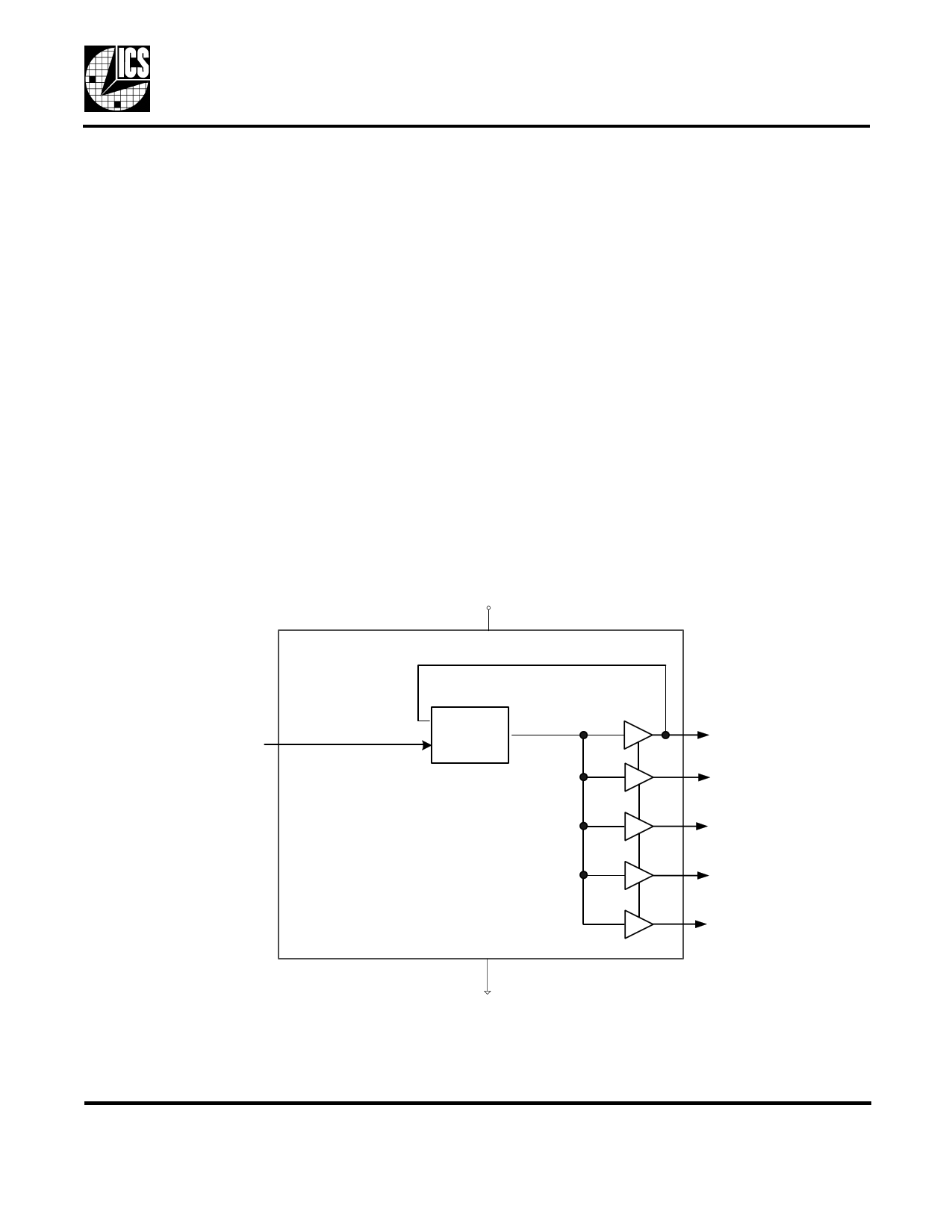
Description
The ICS2305 is a low phase noise, high-speed PLL
based, low-skew zero delay buffer. Based on ICS’
proprietary low jitter Phase Locked Loop (PLL)
techniques, the device provides four low skew outputs
at speeds up to 133 MHz at 3.3 V. The outputs can be
generated from the PLL (for zero delay), or directly
from the input (for testing), and can be set to tri-state
mode or to stop at a low level. The PLL feedback is
on-chip and is obtained from the CLKOUT pad.
The ICS2305 is available in two different versions. The
ICS2305-1 is the base part. The ICS2305-1H is a high
drive version with faster rise and fall times.
Block Diagram
Features
• Clock outputs from 10 to 133 MHz
• Zero input-output delay
• Four low skew (<250 ps) outputs
• Device-to-device skew <700 ps
• Full CMOS outputs with 25 mA output drive
capability at TTL levels
• 5 V tolerant CLKIN
• Tri-state mode for board-level testing
• Advanced, low power, sub-micron CMOS process
• Operating voltage of 3.3 V
• Industrial temperature range available
• Packaged in 8-pin SOIC
• Available in Pb (lead ) free package
VDD
CLKIN
PLL
GND
CLKOUT
CLK1
CLK2
CLK3
CLK4
MDS 2305 D
1
Revision 022505
Integrated Circuit Systems ● 525 Race Street, San Jose, CA 95126 ● tel (408) 297-1201 ● www.icst.com
1 page 
ICS2305
3.3 VOLT ZERO DELAY, LOW SKEW BUFFER
ICS2305M-1H, VDD=3.3 V ±10%, Ambient temperature -40 to +85°C(Industrial), (0-70°C Commercial),
Parameter
Symbol
Conditions
Min. Typ. Max. Units
Output Clock Frequency
Output Clock Frequency
fIN 10 pF load
30 pF load
10 133 MHz
10 100 MHz
Output Rise Time
Output Fall Time
Output Clock Duty Cycle
tOR 0.8 to 2.0 V, outputs loaded
tOF 2.0 to 0.8 V, outputs loaded
tDC measured at 1.4V, Fout=66.67 40
MHz
1.5
1.5
50 60
ns
ns
%
Output Clock Duty Cycle
tDC measured at 1.4V, Fout=50
MHz
45 50 55 %
Device to Device Skew
rising edges at VDD/2
700 ps
Output to Output Skew
rising edges at VDD/2
250 ps
Input to Output Skew
rising edges at VDD/2
±350 ps
Cycle to Cycle Jitter
measured at 66.67M, outputs
loaded
200 ps
PLL Lock Time
Note 3
1.0 ms
Note 3: With VDD at a steady rate and valid input at CLKIN
Thermal Characteristics
Parameter
Symbol Conditions
Thermal Resistance Junction to
Ambient
θJA Still air
θJA 1 m/s air flow
θJA 3 m/s air flow
Thermal Resistance Junction to Case θJC
Min.
Typ.
120
115
105
58
Max.
Units
°C/W
°C/W
°C/W
°C/W
MDS 2305 D
5
Revision 022505
Integrated Circuit Systems ● 525 Race Street, San Jose, CA 95126 ● tel (408) 297-1201 ● www.icst.com
5 Page | ||
| Páginas | Total 8 Páginas | |
| PDF Descargar | [ Datasheet ICS2305.PDF ] | |
Hoja de datos destacado
| Número de pieza | Descripción | Fabricantes |
| ICS2305 | 3.3 VOLT ZERO DELAY / LOW SKEW BUFFER | Integrated Circuit Systems |
| ICS2309 | 3.3 VOLT ZERO DELAY / LOW SKEW BUFFER | Integrated Circuit Systems |
| Número de pieza | Descripción | Fabricantes |
| SLA6805M | High Voltage 3 phase Motor Driver IC. |
Sanken |
| SDC1742 | 12- and 14-Bit Hybrid Synchro / Resolver-to-Digital Converters. |
Analog Devices |
|
DataSheet.es es una pagina web que funciona como un repositorio de manuales o hoja de datos de muchos de los productos más populares, |
| DataSheet.es | 2020 | Privacy Policy | Contacto | Buscar |