|
|
|
PDF ICS2510C Data sheet ( Hoja de datos )
| Número de pieza | ICS2510C | |
| Descripción | 3.3V Phase-Lock Loop Clock Driver | |
| Fabricantes | Integrated Circuit Systems | |
| Logotipo | ||
Hay una vista previa y un enlace de descarga de ICS2510C (archivo pdf) en la parte inferior de esta página. Total 7 Páginas | ||
|
No Preview Available !
Integrated
Circuit
Systems, Inc.
ICS2510C
3.3V Phase-Lock Loop Clock Driver
General Description
Features
The ICS2510C is a high performance, low skew, low jitter • Meets or exceeds PC133 registered DIMM
clock driver. It uses a phase lock loop (PLL) technology to
specification1.1
align, in both phase and frequency, the CLKIN signal with
the CLKOUT signal. It is specifically designed for use with
synchronous SDRAMs. The ICS2510C operates at 3.3V VCC
•
•
Spread Spectrum Clock Compatible
Distributes one clock input to one bank of ten outputs
and drives up to ten clock loads.
• Operating frequency 25MHz to 175MHz
One bank of ten outputs provide low-skew, low-jitter copies
of CLKIN. Output signal duty cycles are adjusted to 50
percent, independent of the duty cycle at CLKIN. Outputs
•
•
External feedback input (FBIN) terminal is used to
synchrionize the outputs to the clock input
No external RC network required
can be enabled or disabled via control (OE) inputs. When the • Operates at 3.3V Vcc
OE inputs are high, the outputs align in phase and frequency
with CLKIN; when the OE inputs are low, the outputs are
•
Plastic 24-pin 173mil TSSOP package
disabled to the logic low state.
The ICS2510C does not require external RC filter
components. The loop filter for the PLL is included on-chip,
minimizing component count, board space, and cost. The test
mode shuts off the PLL and connects the input directly to the
output buffer. This test mode, the ICS2510C can be use as
low skew fanout clock buffer device. The ICS2510C comes
in 24 pin 173mil Thin Shrink Small-Outline package (TSSOP)
package.
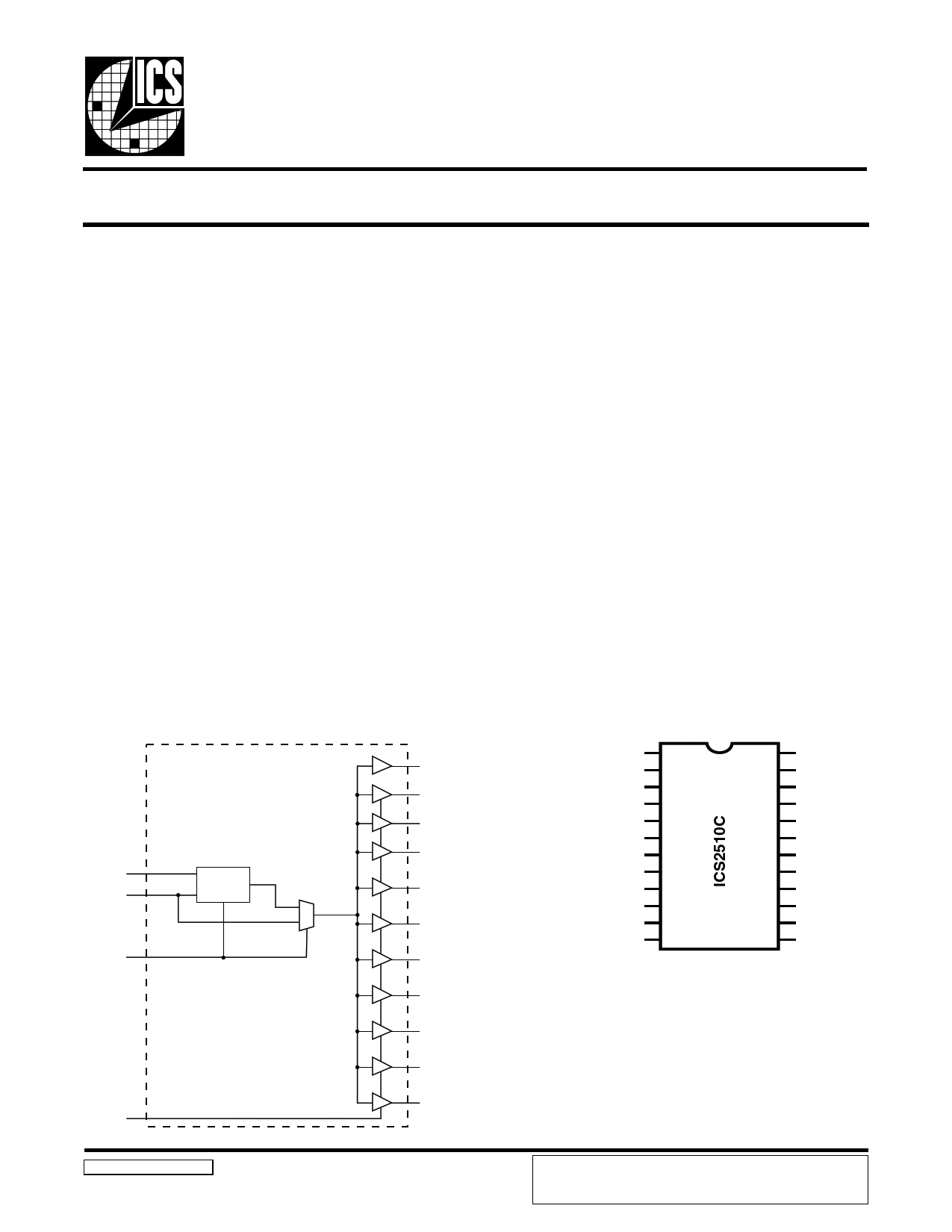
Block Diagram
FBIN
CLKIN
AVCC
PLL
OE
2510 C Rev D 06/15/01
FBOUT
CLK0
CLK1
CLK2
CLK3
CLK4
CLK5
CLK6
CLK7
CLK8
CLK9
Pin Configuration
AGND
VCC
CLK0
CLK1
CLK2
GND
GND
CLK3
CLK4
VCC
OE
FBOUT
1
2
3
4
5
6
7
8
9
10
11
12
24 CLKIN
23 AVCC
22 VCC
21 CLK9
20 CLK8
19 GND
18 GND
17 CLK7
16 CLK6
15 CLK5
14 VCC
13 FBIN
24 Pin TSSOP
4.40 mm. Body, 0.65 mm. pitch
ICS reserves the right to make changes in the device data identified in
this publication without further notice. ICS advises its customers to
obtain the latest version of all device data to verify that any
information being relied upon by the customer is current and accurate.
1 page 
ICS2510C
PARAMETER MEASUREMENT INFORMATION
From Output
Under Test
30 pF 500 Ω
Figure 1. Load Circuit for Outputs
Notes:
1. CL includes probe and jig capacitance.
2. All input pulses are supplied by generators having the following
Figure 2. VoltageWaveforms
Propagation DelayTimes
characteristics: PRR ≤ 133MHz, ZO = 5 0 Ω, Tr ≤1.2ns, Tf ≤1.2ns.
3. The outputs are measured one at a time with one transition per measurement.
Figure 3. Phase Error and Skew Calculations
5
5 Page | ||
| Páginas | Total 7 Páginas | |
| PDF Descargar | [ Datasheet ICS2510C.PDF ] | |
Hoja de datos destacado
| Número de pieza | Descripción | Fabricantes |
| ICS2510C | 3.3V Phase-Lock Loop Clock Driver | Integrated Circuit Systems |
| Número de pieza | Descripción | Fabricantes |
| SLA6805M | High Voltage 3 phase Motor Driver IC. |
Sanken |
| SDC1742 | 12- and 14-Bit Hybrid Synchro / Resolver-to-Digital Converters. |
Analog Devices |
|
DataSheet.es es una pagina web que funciona como un repositorio de manuales o hoja de datos de muchos de los productos más populares, |
| DataSheet.es | 2020 | Privacy Policy | Contacto | Buscar |