|
|
|
PDF IDT72V70800 Data sheet ( Hoja de datos )
| Número de pieza | IDT72V70800 | |
| Descripción | 3.3 VOLT TIME SLOT INTERCHANGE DIGITAL SWITCH 512 x 512 | |
| Fabricantes | Integrated Device Technology | |
| Logotipo | ||
Hay una vista previa y un enlace de descarga de IDT72V70800 (archivo pdf) en la parte inferior de esta página. Total 21 Páginas | ||
|
No Preview Available !
3.3 VOLT TIME SLOT INTERCHANGE
DIGITAL SWITCH
512 x 512
IDT72V70800
FEATURES:
• 512 x 512 channel non-blocking switching at 8.192 Mb/s
• Per-channel variable or constant throughput delay
• Automatic identification of ST-BUS®/GCI interfaces
• Accepts 4 Serial Data Streams of 8.192 Mb/s
• Automatic frame offset delay measurement
• Per-stream frame delay offset programming
• Per-channel high impedance output control
• Per-channel Processor Mode
• Control interface compatible to Intel/Motorola CPUs
• Connection memory block programming
•· Available in 64-pin Thin Plastic Quad Flatpack (TQFP) and
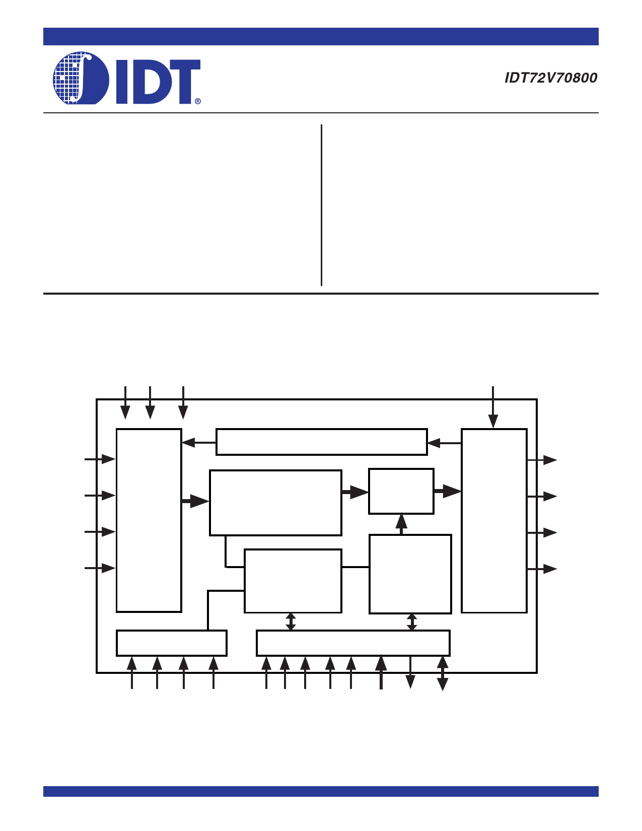
FUNCTIONAL BLOCK DIAGRAM
64-pin Small Thin Quad Flatpack (STQFP)
• 3.3V Power Supply
• Operating Temperature Range -40°C to +85°C
• 3.3V I/O with 5V Tolerant Inputs
DESCRIPTION:
The IDT72V70800 is a non-blocking digital switch that has a capacity of
512 x 512 channels at a serial bit rate of 8.192 Mb/s. Some of the main features
are: programmable stream and channel control, Processor Mode, input offset
delay and high-impedance output control.
Per-stream input delay control is provided for managing large multi-chip
switches that transport both voice channel and concatenated data channels. In
addition, input streams can be individually calibrated for input frame offset.
VCC GND RESET
ODE
RX0
RX1
Receive
Serial Data
RX2 Streams
RX3
Loopback
Data Memory
Internal
Registers
Output
MUX
Connection
Memory
Transmit
Serial Data
Streams
TX0
TX1
TX2
TX3
Timing Unit
Microprocessor Interface
CLK F0i FE/ WFPS
HCLK
AS/ IM DS/ CS R/W/ A0-A7 DTA D8-D15/
ALE RD
WR
AD0-AD7
5709 drw01
IDT and the IDT logo are registered trademarks of Integrated Device Technology, Inc. The ST-BUS is a trademark of Mitel Corp.
1
2003 Integrated Device Technology, Inc. All rights reserved. Product specifications subject to change without notice.
MARCH 2003
DSC-5709/4
1 page 
IDT72V70800 3.3V TIME SLOT INTERCHANGE
DIGITAL SWITCH 512 x 512
COMMERCIALTEMPERATURERANGE
clock(CLK)periodsforwardwithresolutionof½ clockperiod.Theoutputframe
offset cannot be offset or adjusted. See Figure 5, Table 8 and 9 for delay offset
programming.
SERIAL INPUT FRAME ALIGNMENT EVALUATION
The IDT72V70800 provides the frame evaluation (FE) input to determine
different data input delays with respect to the frame pulse F0i.
A measurement cycle is started by setting the start frame evaluation (SFE)
bit low for at least one frame. When the SFE bit in the IMS register is changed
from low to high, the evaluation starts. Two frames later, the complete frame
evaluation (CFE) bit of the frame alignment register (FAR) changes from low
to high to signal that a valid offset measurement is ready to be read from bits 0
to 11 of the FAR register. The SFE bit must be set to zero before a new
measurement cycle started.
In ST-BUS® mode, the falling edge of the frame measurement signal (FE)
is evaluated against the falling edge of the ST-BUS® frame pulse. In GCI mode,
the rising edge of FE is evaluated against the rising edge of the GCI frame pulse.
See Table 7 & Figure 4 for the description of the frame alignment register.
This feature is not available when the WFP Frame Alignment mode is
enabled (i.e., when the WFPS pin is connected to VCC).
MEMORY BLOCK PROGRAMMING
The IDT72V70800 provides users with the capability of initializing the entire
connection memory block in two frames. To set bits 11 to 15 of every connection
memory location, first program the desired pattern in bits 5 to 9 of the IMS register.
The block programming mode is enabled by setting the memory block
program (MBP) bit of the control register high. When the block programming
enable (BPE) bit of the IMS register is set to high, the block programming data
will be loaded into the bits 11 to 15 of every connection memory location. The
other connection memory bits (bit 0 to bit 10) are loaded with zeros. When the
memory block programming is complete, the device resets the BPE bit to zero.
LOOPBACK CONTROL
The loopback control (LPBK) bit of each connection memory location allows
the TX output data to be looped backed internally to the RX input for diagnostic
purposes.
If the LPBK bit is high, the associated TX output channel data is internally
looped back to the RX input channel (i.e., data from TX n channel m routes to
the RX n channel m internally); if the LPBK bit is low, the loopback feature is
disabled. For proper per-channel loopback operation, the contents of frame
delay offset registers must be set to zero.
DELAY THROUGH THE IDT72V70800
The switching of information from the input serial streams to the output serial
streams results in a throughput delay. The device can be programmed to
perform time-slot interchange functions with different throughput delay capabili-
ties on the per-channel basis. For voice applications, variable throughput delay
is best as it ensures minimum delay between input and output data. In wideband
data applications, constant throughput delay is best as the frame integrity of the
information is maintained through the switch.
The delay through the device varies according to the type of throughput
delay selected in the V/C bit of the connection memory.
VARIABLE DELAY MODE (V/C BIT = 0)
In this mode, the delay is dependent only on the combination of source and
destination channels and is independent of input and output streams. The
minimum delay achievable in the IDT72V70800 is three time-slots. If the input
channel data is switched to the same output channel (channel n, frame p), it will
be output in the following frame (channel n, frame p+1). The same is true if input
channel n is switched to output channel n+1 or n+2. If the input channel n is
switched to output channel n+3, n+4,..., the new output data will appear in the
same frame. Table 1 shows the possible delays for the IDT72V70800 in the
variable delay mode.
CONSTANT DELAY MODE (V/C BIT = 1)
In this mode, frame integrity is maintained in all switching configurations by
making use of a multiple data memory buffer. Input channel data is written into
the data memory buffers during frame n will be read out during frame n+2. In
the IDT72V70800, the minimum throughput delay achievable in the constant
delaymodewillbeoneframe. SeeTable2forpossibledelaysinconstantdelay
mode.
MICROPROCESSOR INTERFACE
The IDT72V70800 provides a parallel microprocessor interface for multi-
plexed or non-multiplexed bus structures. This interface is compatible with
Motorola non-multiplexed and multiplexed buses.
If the IM pin is low a Motorola non-multiplexed bus should be connected to
the device. If the IM pin is high, the device monitors the AS/ALE and DS/RD to
determine what mode the IDT72V70800 should operate in.
If DS/RD is low at the rising edge of AS/ALE, then the mode 1 multiplexed
timing is selected. If DS/RD is high at the rising edge of AS/ALE, then the mode
2 multiplexed bus timing is selected.
For multiplexed operation, the required signals are the 8-bit data and
address (AD0-AD7), 8-bit Data (D8-D15), Address strobe/Address latch
enable(AS/ALE),Datastrobe/Read(DS/RD),Read/Write/Write(R/W /WR),
Chip select (CS) and Data transfer acknowledge (DTA). See Figure 12 and
Figure 13 for multiplexed parallel microport timing.
For the Motorola non-multiplexed bus, the required signals are the 16-bit
data bus (AD0-AD7, D8-D15), 8-bit address bus (A0-A7) and 4 control lines
(CS, DS, R/W and DTA). See Figure 14 and 15 for Motorola non-multiplexed
microport timing.
The IDT72V70800 microport provides access to the internal registers,
connection and data memories. All locations provide read/write access except
for the data memory and the frame alignment register which are read only.
MEMORY MAPPING
The address bus on the microprocessor interface selects the internal
registers and memories of the IDT72V70800.
If the A7 address input is low, then A6 through A0 are used to address the
interface mode selection (IMS), control (CR), frame alignment (FAR) and frame
input offset (FOR) registers (Table 4). If the A7 is high, then A6 through A0 are
used to select 128 locations corresponding to data rate of the ST-BUS®. The
address input lines and the stream address bits (STA) of the control register allow
access to the entire data and connection memories. The control and IMS
registers together control all the major functions of the device, see Figure 3.
As explained in the Serial Data Interface Timing and Switching Configura-
tions sections, after system power-up, the IMS register should be programmed
immediately to establish the desired switching configuration.
The data in the control register consists of the memory block programming
bit (MBP), the memory select bit (MS) and the stream address bits (STA). As
explained in the Memory Block Programming section, the MBP bit allows the
entire connection memory block to be programmed. The memory select bit is
5
5 Page 
IDT72V70800 3.3V TIME SLOT INTERCHANGE
DIGITAL SWITCH 512 x 512
COMMERCIALTEMPERATURERANGE
TABLE 9 — OFFSET BITS (OFn2, OFn1, OFn0, DLEn) & FRAME DELAY BITS
(FD11, FD2-0)
Input Stream
Offset
No clock period shift (Default)
+ 0.5 clock period shift
+ 1.0 clock period shift
+ 1.5 clock period shift
+ 2.0 clock period shift
+ 2.5 clock period shift
+ 3.0 clock period shift
+ 3.5 clock period shift
+ 4.0 clock period shift
+ 4.5 clock period shift
FD11
1
0
1
0
1
0
1
0
1
0
Measurement Result from
Frame Delay Bits
FD2 FD1 FD0
000
000
001
001
010
010
011
011
100
100
OFn2
0
0
0
0
0
0
0
0
1
1
Corresponding
OffsetBits
OFn1
0
0
0
0
1
1
1
1
0
0
OFn0
0
0
1
1
0
0
1
1
0
0
DLEn
0
1
0
1
0
1
0
1
0
1
ST-BUS F0i
CLK
RX Stream
RX Stream
RX Stream
RX Stream
GCI F0i
CLK
RX Stream
RX Stream
RX Stream
RX Stream
Bit 7
Bit 7
Bit 7
Bit 7
offset = 0, DLE = 0
offset = 1, DLE = 0
offset = 0, DLE = 1
offset = 1, DLE = 1
denotes the 3/4 point of the bit cell
Bit 0
Bit 0
Bit 0
Bit 0
offset = 0, DLE = 0
offset = 1, DLE = 0
offset = 0, DLE = 1
offset = 1, DLE = 1
denotes the 3/4 point of the bit cell
Figure 5. Examples for Input Offset Delay Timing
11
5709 drw05
11 Page | ||
| Páginas | Total 21 Páginas | |
| PDF Descargar | [ Datasheet IDT72V70800.PDF ] | |
Hoja de datos destacado
| Número de pieza | Descripción | Fabricantes |
| IDT72V70800 | 3.3 VOLT TIME SLOT INTERCHANGE DIGITAL SWITCH 512 x 512 | Integrated Device Technology |
| Número de pieza | Descripción | Fabricantes |
| SLA6805M | High Voltage 3 phase Motor Driver IC. |
Sanken |
| SDC1742 | 12- and 14-Bit Hybrid Synchro / Resolver-to-Digital Converters. |
Analog Devices |
|
DataSheet.es es una pagina web que funciona como un repositorio de manuales o hoja de datos de muchos de los productos más populares, |
| DataSheet.es | 2020 | Privacy Policy | Contacto | Buscar |