|
|
PDF FAS368M Data sheet ( Hoja de datos )
| Número de pieza | FAS368M | |
| Descripción | Fast Architecture SCSI Precossor | |
| Fabricantes | QLogic | |
| Logotipo |  |
|
Hay una vista previa y un enlace de descarga de FAS368M (archivo pdf) en la parte inferior de esta página. Total 8 Páginas | ||
|
No Preview Available !
.com QLogic Corporation
ww.DFatAaSSh3e6e8t4MU Fast ArDchatiateShceteutre SCSI ProcessorFeatures
w s Compliance with ANSI X3T10/1142D SCSI
mParallel Interconnect-2 (SPI-2) standard
s Compliance with ANSI SCSI configured
oautomatically (SCAM) protocol levels 1 and 2
.cs Sustained SCSI data transfer rates of up to:
Ì 40 Mbytes/sec synchronous (Ultra and wide
SCSI)
UÌ 14 Mbytes/sec asynchronous (wide SCSI)
s Synchronous DMA timing; DMA speed of
t450 Mbytes/sec
s REQ and ACK programmable assertion and
edeassertion control
s Support for hot plugging
es Target and initiator block transfer sequences
s Bus idle timer
hs Split-bus architecture
Ss Pipelined command structure
s On-chip, single-ended SCSI transceivers
ta(48-mA drivers)
s On-chip, multimode, low voltage differential
(LVD) drivers
as On-chip differential sense decoder
s Initiator and target roles
.Ds Active negation
s 16-bit recommand counter
s Differential mode
ws SCSI bus reset watchdog timer
wProduct Description
mThe FAS368M is a new addition to the QLogic fast
w oarchitecture SCSI processor (FAS) chip family. The
.cFAS368M supports internal multimode LVD and
Usingle-ended (SE) transceivers, which allow the chip to
t4support LVD and SE operations in initiator and target roles.
eThe FAS368M is a single-chip controller for use in host
eand peripheral applications. To ensure firmware
hcompatibility and provide FAS366U customers a seamless
Supgrade path, the FAS368M uses the same SCSI core,
tafoundry, and process as the FAS366U. Note that the
FAS368M package size, pin out, and transceivers differ
from the FAS366U. The FAS368M block diagram is shown
in figure 1.
The FAS368M implements QLogic’s new SCSI target
and initiator block transfer sequences. The block sequences
reduce firmware overhead and are composed of the
following new commands: Target Block Sequence
(including the bus idle timer), Initiator Block Sequence,
Load/Unload Block Registers sequences, Abort Block
Sequence, and Disconnect Abort Block Sequence.
The FAS368M supports both single-ended and
differential mode SCSI operations and operates in initiator
and target roles. The FAS368M has been optimized for
interaction with a DMA controller and the controlling
microprocessor.
The versatile split-bus architecture supports various
microprocessor and DMA bus configurations. A separate
8-bit microprocessor bus (PAD) provides access to all
internal registers, and a 16-bit DMA bus (DB) provides a
path for DMA transfers through the FIFO. Each bus is
protected by a parity bit (byte-wide parity) to improve data
integrity. During data transfer, the microprocessor has
instant access to status and has the ability to execute
commands.
SCAM Implementation
The FAS368M supports levels 1 and 2 of the SCAM
protocol. Refer to the latest revision of X3T10/855D,
Annex B. The SCAM protocol requires direct access and
control over the SCSI data bus and several of the SCSI
phase and control signals. The majority of the SCAM
protocol can be implemented in firmware at
microprocessor speeds. The following SCAM features are
supported in the hardware:
s Arbitration without an ID
s Slow response to selection with an unconfirmed ID
s Detection of and response to SCAM selection
www.Da53368-580-00 A
FAS368M
1
1 page 
QLogic Corporation
Packaging
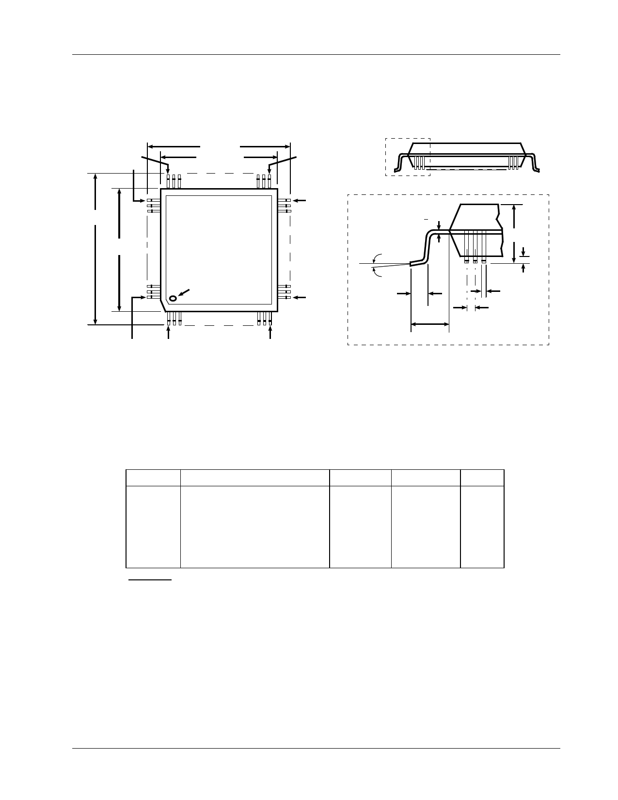
The FAS368M is available in a 144-pin thin quad flat pack (TQFP). The mechanical drawings are illustrated in figure 3.
PIN 108
PIN 109
22.0 ± 0.4
20.0 ± 0.2
22.0 ± 0.4
20.0 ± 0.2
PIN 73
PIN72
SEE DETAIL A
0.10 + 0.05
4° TYPICAL
1.6 MAX
INDEX MARK
PIN 37
0.5 ± 0.2
1.0 ± 0.2
NOTE:
PIN 144
PIN 1
PIN 36
ALL DIMENSIONS ARE IN MILLIMETERS.
ALL DIMENSIONS ARE NOMINAL UNLESS SPECIFIED OTHERWISE.
Figure 3. FAS368M Mechanical Drawings
DETAIL A
0.1 ± 0.1
0.2 ± 0.1
0.5
Electrical Characteristics
Table 4. Operating Conditions
Symbol
Description
Minimum
Maximum
Unit
VDD Supply voltage (5 volt)
4.75 5.25 V
VDD
IDDa
IDDb
Supply voltage (3 volt)
Supply current (static IDD)
Supply current (dynamic IDD)
3.3 V - 5%
3.3 V + 5%
1
TBD
V
mA
mA
TA Ambient temperature
0 70 oC
Table Notes
Conditions that not within the operating conditions but within the absolute maximum stress ratings may
cause the chip to malfunction.
Capacitance in and out (CIN, COUT) is 15 pF maximum for all pins.
aStatic IDD is measured with no clocks running and all inputs forced to VDD, all outputs unloaded, all
bidirectional pins configured as inputs, and LVD mode disabled.
bDynamic IDD is dependent on the application.
53368-580-00 A
FAS368M
5
5 Page | ||
| Páginas | Total 8 Páginas | |
| PDF Descargar | [ Datasheet FAS368M.PDF ] | |
Hoja de datos destacado
| Número de pieza | Descripción | Fabricantes |
| FAS368M | Fast Architecture SCSI Precossor | QLogic |
| Número de pieza | Descripción | Fabricantes |
| SLA6805M | High Voltage 3 phase Motor Driver IC. |
Sanken |
| SDC1742 | 12- and 14-Bit Hybrid Synchro / Resolver-to-Digital Converters. |
Analog Devices |
|
DataSheet.es es una pagina web que funciona como un repositorio de manuales o hoja de datos de muchos de los productos más populares, |
| DataSheet.es | 2020 | Privacy Policy | Contacto | Buscar |
