|
|
PDF 3851031403BCB Data sheet ( Hoja de datos )
| Número de pieza | 3851031403BCB | |
| Descripción | M38510/31403B | |
| Fabricantes | Sarnoff | |
| Logotipo |  |
|
Hay una vista previa y un enlace de descarga de 3851031403BCB (archivo pdf) en la parte inferior de esta página. Total 30 Páginas | ||
|
No Preview Available !
INCH-POUND
MIL-M-38510/314C
14 July 2003 __
SUPERSEDING
MIL-M-38510/314B
23 May 1978
MILITARY SPECIFICATION
MICROCIRCUITS, DIGITAL, LOW-POWER SCHOTTKY, TTL, MONOSTABLE
MULTIVIBRATORS, MONOLITHIC SILICON
Inactive for new design after 18 April 1997.
www.DataSheet4U.com
1. SCOPE
This specification is approved for use by all Departments
and Agencies of the Department of Defense.
1.1 Scope. This specification covers the detail requirements for monolithic silicon, low-power Schottky TTL,
monostable multivibrator microcircuits. Two product assurance classes and a choice of case outlines and lead
finishes are provided for each type and are reflected in the complete part number. For this product, the requirements
of MIL-M-38510 have been superseded by MIL-PRF-38535, (see 6.3).
1.2 Part number. The part number should be in accordance with MIL-PRF-38535, and as specified herein.
1.2.1 Device types. The device types should be as follows:
Device type
01
02
03
Circuit
Dual monostable multivibrator, retriggerable, with clear
Dual monostable multivibrator, Schmitt trigger inputs, with clear
Single monostable multivibrator, retriggerable, with clear
1.2.2 Device class. The device class should be the product assurance level as defined in MIL-PRF-38535.
1.2.3 Case outlines. The case outlines should be as designated in MIL-STD-1835 and as follows:
Outline letter
Descriptive designator
Terminals
Package style
A GDFP5-F14 or CDFP6-F14
B GDFP4-14
C GDIP1-T14 or CDIP2-T14
D GDFP1-F14 or CDFP2-F14
E GDIP1-T16 or CDIP2-T16
F GDFP2-F16 or CDFP3-F16
2 CQCC1-N20
14 Flat pack
14 Flat pack
14 Dual-in-line
14 Flat pack
16 Dual-in-line
16 Flat pack
20 Square leadless chip carrier
.comBeneficial comments (recommendations, additions, deletions) and any pertinent data which may be of use in
uimproving this document should be addressed to: Commander, Defense Supply Center Columbus, ATTN:
t4DSCC-VAS, P. O. Box 3990, Columbus, OH 43216-5000, by using the self addressed Standardization
eDocument Improvement Proposal (DD Form 1426) appearing at the end of this document or by letter.
heAMSC N/A
www.datasDISTRIBUTION STATEMENT A. Approved for public release; distribution is unlimited.
FSC 5962
1 page 
Test
High level output voltage
Low level output voltage
Input clamp voltage
www.DataSheet4U.com
Low level input current
MIL-M-38510/314C
TABLE I. Electrical performance characteristics.
Symbol
VOH
VOL
VIC
IIL1
Conditions
-55°C ≤ TC ≤ +125°C
unless otherwise specified
VCC = 4.5 V, VIL = 0.7 V,
VIH = 2.0 V, IOH = -400 µA
VCC = 4.5 V, VIL = 0.7 V,
VIH = 2.0 V, IOL = 4 mA
VCC = 4.5 V, IIN = -18 mA,
TC = +25°C
VCC = 5.5 V, VIN = 0.4 V
Device
types
All
All
All
01, 03
Limits
Min Max
2.5
0.4
-1.5
-160 -400
Unit
V
V
V
µA
Low level input current
at clear input
Low level input current at AIN
IIL2
02 -30 -680
02 -30 -400
Low level input current BIN
02 -30 -580
High level input current
IIH1 VCC = 5.5 V, VIN = 2.7 V
All
20 µA
High level input current
IIH2 VCC = 5.5 V, VIN = 5.5 V
All 100
Short circuit output current
Supply current (quiescent)
IOS
ICC1
VCC = 5.5 V, VIH = 5.5 V,
VIL = GND
VCC = 5.5 V
All
-15 -130
mA
02 11 mA
Supply current (quiescent or
triggered)
Supply current (triggered)
ICC2
ICC3
01 20
03 11
02 27
Propagation delay time low to
high level from input A
Propagation delay time low to
high level from input B
Propagation delay time low to
high level from clear
Propagation delay time
high to low level from input A
tPLH1
tPLH2
tPLH3
tPHL1
See footnotes at end of table.
VCC = 5.0 V
CL = 50 pF ±5%, RL = 2 kΩ ±5%
Cext = 1/
Rext = 1/
01, 03
02
01, 03
02
01, 03
02
01, 03
02
5 57
5 113
5 74
5 90
5 75
5 105
5 75
5 128
ns
5
5 Page 
www.DataSheet4U.com
MIL-M-38510/314C
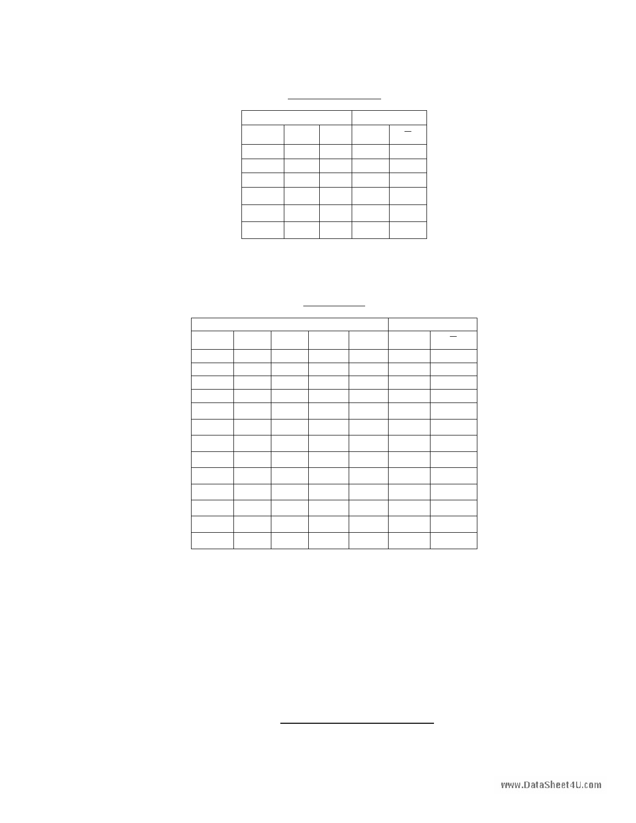
Device type 01 and 02
INPUTS
CLEAR A
LX
XH
XX
HL
H↓
↑L
B
X
X
L
↑
H
H
OUTPUTS
QQ
LH
LH
LH
┌┐ └┘
┌┐ └┘
┌┐ └┘
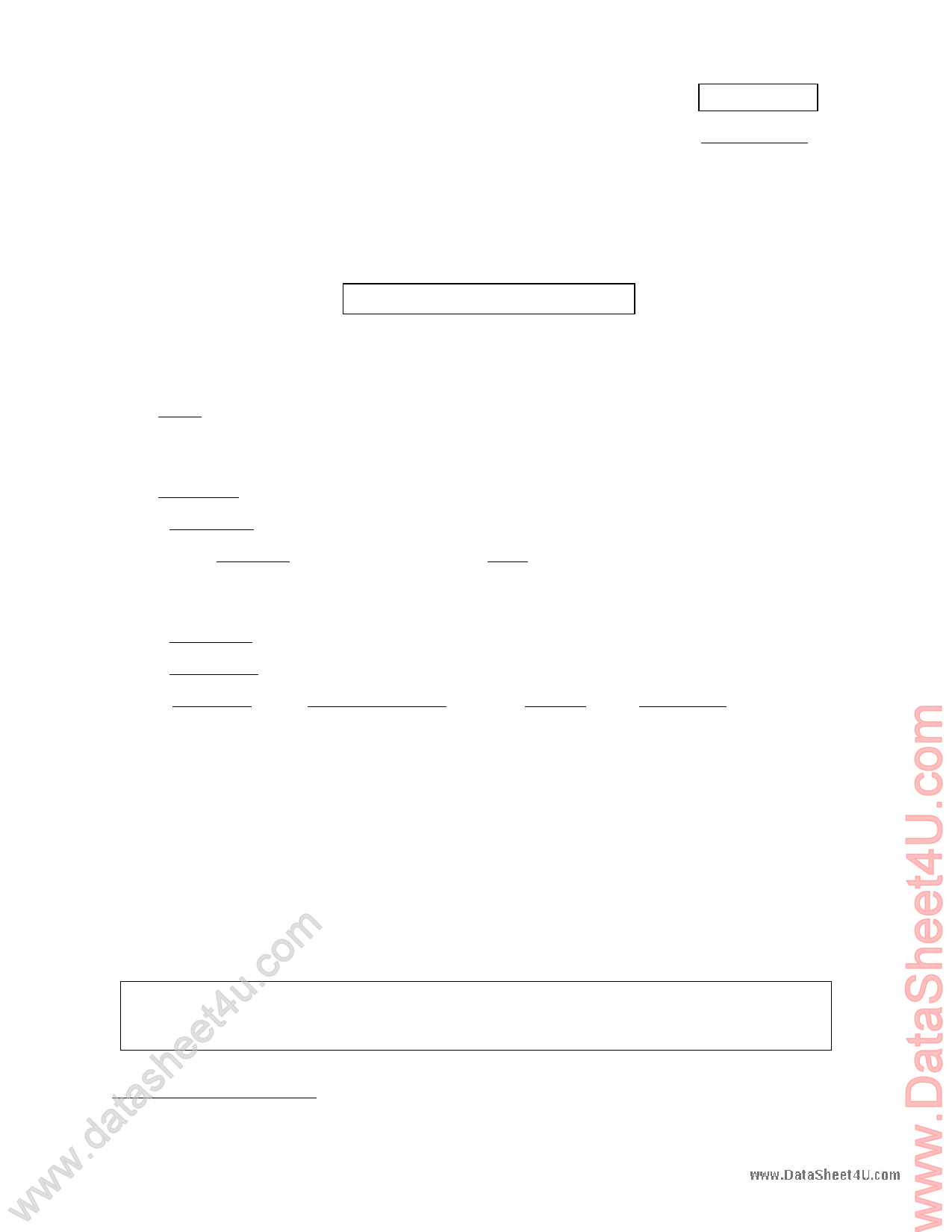
Device type 03
INPUTS
OUTPUTS
CLEAR A1
A2
B1
B2
Q
Q
L XX X X L
H
X HH X X L
H
X XX L X L
H
X XX X L L
H
H L X ↑ H ┌┐ └┘
H L X H ↑ ┌┐ └┘
H X L ↑ H ┌┐ └┘
H X L H ↑ ┌┐ └┘
H H ↓ H H ┌┐ └┘
H ↓ ↓ H H ┌┐ └┘
H ↓ H H H ┌┐ └┘
↑ L X H H ┌┐ └┘
↑ X L H H ┌┐ └┘
NOTES:
1. H = high level (steady state), L = low level (steady state), ↑ = transition from low to high level,
↓ = transition from high to low level, ┌┐ = one high level pulse, └┘ = one low level pulse,
X = irrelevant (any input, including transitions).
2. To use the internal timing resistor of device type 03 connect Rint to VCC.
3. An external timing capacitor may be connected between Cext and Rext/Cext (positive).
4. For accurate repeatable pulse widths, connect an external resistor between Rext/Cext and
VCC with Rint open circuited.
5. To obtain variable pulse widths, connect external variable resistance between Rint or Rext/Cext and VCC.
FIGURE 2. Truth table and functional description.
11
11 Page | ||
| Páginas | Total 30 Páginas | |
| PDF Descargar | [ Datasheet 3851031403BCB.PDF ] | |
Hoja de datos destacado
| Número de pieza | Descripción | Fabricantes |
| 3851031403BCB | M38510/31403B | Sarnoff |
| Número de pieza | Descripción | Fabricantes |
| SLA6805M | High Voltage 3 phase Motor Driver IC. |
Sanken |
| SDC1742 | 12- and 14-Bit Hybrid Synchro / Resolver-to-Digital Converters. |
Analog Devices |
|
DataSheet.es es una pagina web que funciona como un repositorio de manuales o hoja de datos de muchos de los productos más populares, |
| DataSheet.es | 2020 | Privacy Policy | Contacto | Buscar |
