|
|
|
PDF ADC14L020 Data sheet ( Hoja de datos )
| Número de pieza | ADC14L020 | |
| Descripción | 14-Bit 20 MSPS / 150mW A/D Converter | |
| Fabricantes | National Semiconductor | |
| Logotipo | ||
Hay una vista previa y un enlace de descarga de ADC14L020 (archivo pdf) en la parte inferior de esta página. Total 23 Páginas | ||
|
No Preview Available !
August 2005
ADC14L020
14-Bit, 20 MSPS, 150 mW A/D Converter
General Description
The ADC14L020 is a low power monolithic CMOS analog-
to-digital converter capable of converting analog input sig-
nals into 14-bit digital words at 20 Megasamples per second
(MSPS). This converter uses a differential, pipeline architec-
ture with digital error correction and an on-chip sample-and-
hold circuit to minimize power consumption while providing
excellent dynamic performance and a 150 MHz Full Power
Bandwidth. Operating on a single +3.3V power supply, the
ADC14L020 achieves 12.0 effective bits at nyquist and con-
sumes just 150 mW at 20 MSPS . The Power Down feature
reduces power consumption to 15 mW.
The differential inputs provide a full scale differential input
swing equal to 2 times VREF with the possibility of a single-
ended input. Full use of the differential input is recom-
mended for optimum performance. Duty cycle stabilization
and output data format are selectable using a quad state
function pin. The output data can be set for offset binary or
two’s complement.
To ease interfacing to lower voltage systems, the digital
output driver power pins of the ADC14L020 can be con-
nected to a separate supply voltage in the range of 2.4V to
the analog supply voltage.
This device is available in the 32-lead LQFP package and
will operate over the industrial temperature range of −40˚C to
+85˚C. An evaluation board is available to ease the evalua-
tion process.
Features
n Single +3.3V supply operation
n Internal sample-and-hold
n Internal reference
n Outputs 2.4V to 3.6V compatible
n Duty Cycle Stabilizer
n Power down mode
Key Specifications
n Resolution
n DNL
n SNR (fIN = 10 MHz)
n SFDR (fIN = 10 MHz)
n Data Latency
n Power Consumption
n -- Operating
n -- Power Down Mode
Applications
n Medical Imaging
n Instrumentation
n Communications
n Digital Video
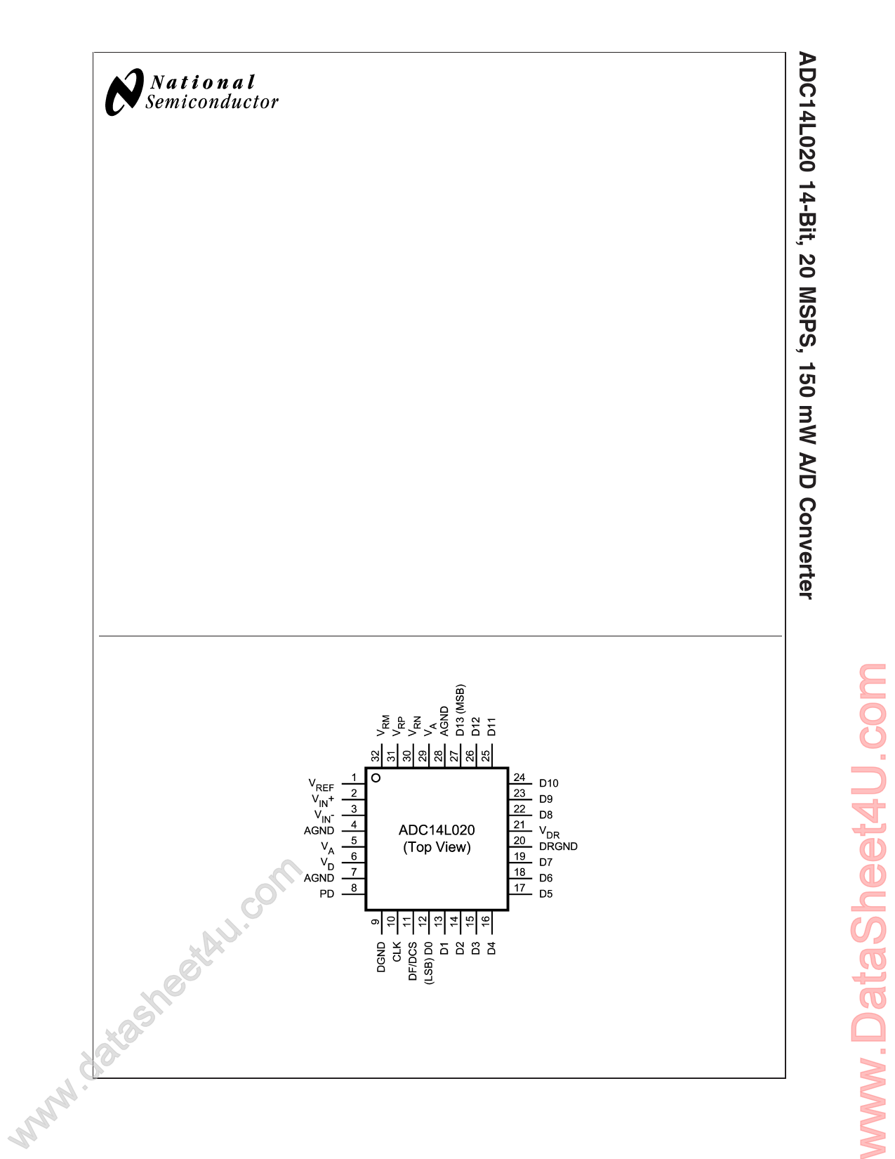
Connection Diagram
14 Bits
±0.5 LSB (typ)
74 dB (typ)
93 dB (typ)
7 Clock Cycles
150 mW (typ)
15 mW (typ)
www.datasheet4u.com© 2005 National Semiconductor Corporation
DS201570
20157001
www.national.com
1 page 
Absolute Maximum Ratings (Notes 1,
2)
If Military/Aerospace specified devices are required,
please contact the National Semiconductor Sales Office/
Distributors for availability and specifications.
VA, VD, VDR
|VA–VD|
Voltage on Any Input or Output Pin
4.2V
≤ 100 mV
−0.3V to (VA or VD
+0.3V)
Input Current at Any Pin (Note 3)
±25 mA
Package Input Current (Note 3)
±50 mA
Package Dissipation at TA = 25˚C
ESD Susceptibility
See (Note 4)
Human Body Model (Note 5)
2500V
Machine Model (Note 5)
250V
Storage Temperature
−65˚C to +150˚C
Soldering process must comply with National
Semiconductor’s Reflow Temperature Profile
specifications. Refer to www.national.com/packaging.
(Note 6)
Operating Ratings (Notes 1, 2)
Operating Temperature
Supply Voltage (VA, VD)
Output Driver Supply (VDR)
CLK, PD
Clock Duty Cycle (DCS On)
Clock Duty Cycle (DCS Off)
Analog Input Pins
VCM
|AGND–DGND|
−40˚C ≤ TA ≤ +85˚C
+3.0V to +3.6V
+2.4V to VD
−0.05V to (VD + 0.05V)
20% to 80%
40% to 60%
0V to 2.6V
0.5V to 2.0V
≤100mV
Converter Electrical Characteristics
Unless otherwise specified, the following specifications apply for AGND = DGND = DR GND = 0V, VA = VD = +3.3V, VDR =
+2.5V, PD = 0V, External VREF = +1.0V, fCLK = 20 MHz, fIN = 10 MHz at -0.5dBFS, tr = tf = 2 ns, CL = 15 pF/pin, Duty Cycle
Stabilizer On. Boldface limits apply for TJ = TMIN to TMAX: all other limits TJ = 25˚C (Notes 7, 8, 9)
Symbol
Parameter
Conditions
Typical Limits
(Note 10) (Note 10)
Units
(Limits)
STATIC CONVERTER CHARACTERISTICS
Resolution with No Missing Codes
14 Bits (min)
INL Integral Non Linearity (Note 11)
±1.4
±3.8
LSB (max)
DNL
Differential Non Linearity
±0.5
±1.0
LSB (max)
PGE
Positive Gain Error
0.3 ±3.3 %FS (max)
NGE
Negative Gain Error
0.3 ±3.3 %FS (max)
TC GE
VOFF
TC
VOFF
Gain Error Tempco
Offset Error (VIN+ = VIN−)
Offset Error Tempco
Under Range Output Code
−40˚C ≤ TA ≤ +85˚C
−40˚C ≤ TA ≤ +85˚C
2.5
-0.06
1.5
±0.85
0
ppm/˚C
%FS (max)
ppm/˚C
Over Range Output Code
16383
REFERENCE AND ANALOG INPUT CHARACTERISTICS
VCM Common Mode Input Voltage
0.5
1.5
2.0
V (min)
V (max)
VRM Reference Output Voltage
Output load = 1 mA
CIN
VIN Input Capacitance (each pin to
GND)
VIN = 1.5 Vdc
± 0.5 V
(CLK LOW)
(CLK HIGH)
1.5
11
4.5
V
pF
pF
VREF
External Reference Voltage (Note
13)
1.00
0.8
1.2
V (min)
V (max)
Reference Input Resistance
1 MΩ (min)
5 www.national.com
5 Page 
Typical Performance Characteristics, DNL, INL Unless otherwise specified, the following
specifications apply for AGND = DGND = DR GND = 0V, VA = VD = +3.3V, VDR = +2.5V, PD = 0V, External VREF = +1.0V,
fCLK = 20 MHz, fIN = 0 MHz, tr = tf = 2 ns, CL = 15 pF/pin, Duty Cycle Stabilizer On. Boldface limits apply for TJ = TMIN to
TMAX: all other limits TJ = 25˚C
DNL
INL
DNL vs. fCLK
20157061
INL vs. fCLK
20157062
DNL vs. Clock Duty Cycle
20157063
INL vs. Clock Duty Cycle
20157064
20157065
11
20157066
www.national.com
11 Page | ||
| Páginas | Total 23 Páginas | |
| PDF Descargar | [ Datasheet ADC14L020.PDF ] | |
Hoja de datos destacado
| Número de pieza | Descripción | Fabricantes |
| ADC14L020 | 14-Bit 20 MSPS / 150mW A/D Converter | National Semiconductor |
| ADC14L020 | ADC14L020 14-Bit 20 MSPS 150 mW A/D Converter (Rev. D) | Texas Instruments |
| Número de pieza | Descripción | Fabricantes |
| SLA6805M | High Voltage 3 phase Motor Driver IC. |
Sanken |
| SDC1742 | 12- and 14-Bit Hybrid Synchro / Resolver-to-Digital Converters. |
Analog Devices |
|
DataSheet.es es una pagina web que funciona como un repositorio de manuales o hoja de datos de muchos de los productos más populares, |
| DataSheet.es | 2020 | Privacy Policy | Contacto | Buscar |