|
|
|
PDF DP8572AM Data sheet ( Hoja de datos )
| Número de pieza | DP8572AM | |
| Descripción | Real Time Clock (RTC) | |
| Fabricantes | National Semiconductor | |
| Logotipo | ||
Hay una vista previa y un enlace de descarga de DP8572AM (archivo pdf) en la parte inferior de esta página. Total 22 Páginas | ||
|
No Preview Available !
May 1993
DP8572A DP8572AM Real Time Clock (RTC)
General Description
The DP8572A (8572AM militarized version) is intended for
use in microprocessor based systems where information is
required for multi-tasking data logging or general time of
day date information This device is implemented in low
voltage silicon gate microCMOS technology to provide low
standby power in battery back-up environments The cir-
cuit’s architecture is such that it looks like a contiguous
block of memory or I O ports The address space is orga-
nized as 2 software selectable pages of 32 bytes This in-
cludes the Control Registers the Clock Counters the Alarm
Compare RAM and the Time Save RAM Any of the RAM
locations that are not being used for their intended purpose
may be used as general purpose CMOS RAM
Time and date are maintained from 1 100 of a second to
year and leap year in a BCD format 12 or 24 hour modes
Day of week day of month and day of year counters are
provided Time is controlled by an on-chip crystal oscillator
requiring only the addition of the crystal and two capacitors
The choice of crystal frequency is program selectable
Power failure logic and control functions have been integrat-
ed on chip This logic is used by the RTC to issue a power
fail interrupt and lock out the mp interface The time power
fails may be logged into RAM automatically when VBB l
VCC Additionally two supply pins are provided When
VBB l VCC internal circuitry will automatically switch from
the main supply to the battery supply Status bits are provid-
ed to indicate initial application of battery power system
power and low battery detect
(Continued)
Features
Y Full function real time clock calendar
12 24 hour mode timekeeping
Day of week and day of years counters
Four selectable oscillator frequencies
Parallel resonant oscillator
Y Power fail features
Internal power supply switch to external battery
Power Supply Bus glitch protection
Automatic log of time into RAM at power failure
Y On-chip interrupt structure
Periodic alarm and power fail interrupts
Y Up to 44 bytes of CMOS RAM
Y MIL-STD-883C compliant
Y SMD 5962-91641-01MJX (future)
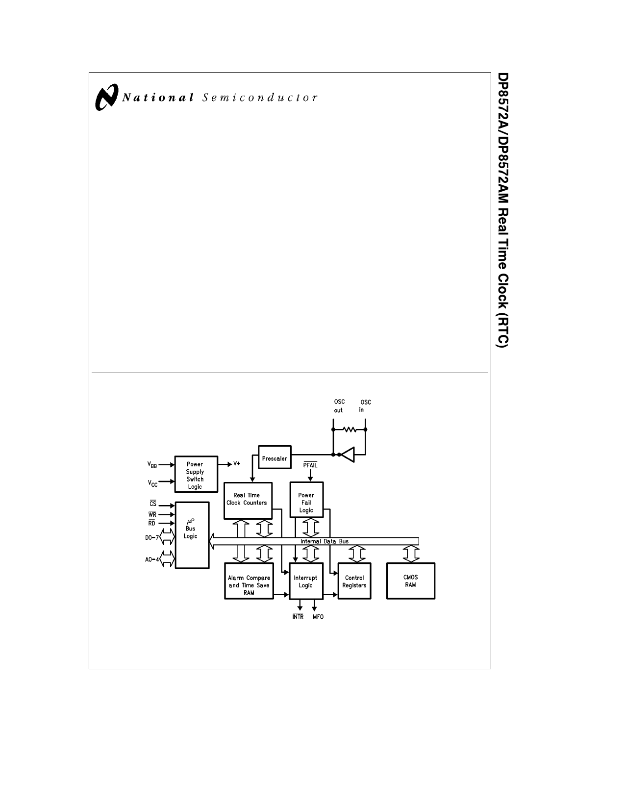
Block Diagram
FIGURE 1
TRI-STATE is a registered trademark of National Semiconductor Corporation
C1995 National Semiconductor Corporation TL F 9980
TL F 9980 – 1
RRD-B30M75 Printed in U S A
1 page 
8572AM Military Version
AC Electrical Characteristics
VCC e 4 5V and 5 5V VBB e 3V VPFAIL l VIH CL e 100 pF (unless otherwise specified)
Symbol
Parameter
Min Max Units
READ TIMING
tAR
tRW
tCD
tRD
tDZ
tRCH
tDS
WRITE TIMING
Address Valid Prior to Read Strobe
Read Strobe Width (Note 8)
Chip Select to Data Valid Time
Read Strobe to Valid Data
Read or Chip Select to TRI-STATE
Chip Select Hold after Read Strobe
Minimum Inactive Time between Read or Write Accesses
20
80
0
50
80
70
60
ns
ns
ns
ns
ns
ns
ns
tAW Address Valid before Write Strobe
20 ns
tCW Chip Select to End of Write Strobe
90 ns
tWW Write Strobe Width (Note 9)
80 ns
tDW Data Valid to End of Write Strobe
50 ns
tWCH
Chip Select Hold after Write Strobe
0 ns
Note 8 Read Strobe width as used in the read timing table is defined as the period when both chip select and read inputs are low Hence read commences when
both signals are low and terminates when either signal returns high
Note 9 Write Strobe width as used in the write timing table is defined as the period when both chip select and write inputs are low Hence write commences when
both signals are low and terminates when either signal returns high
AC Test Conditions
Input Pulse Levels
Input Rise and Fall Times
Input and Output
Reference Levels
TRI-STATE Reference
Levels (Note 11)
GND to 3 0V
6 ns (10%–90%)
1 3V
Active High a0 5V
Active Low b0 5V
Note 10 CL e 100 pF includes jig and scope capacitance
Note 11 S1 e VCC for active low to high impedance measurements
S1 e GND for active high to high impedance measurements
S1 e open for all other timing measurements
Capacitance (TA e 25 C f e 1 MHz)
Symbol
Parameter
(Note 12)
Typ Units
CIN Input Capacitance 5 pF
COUT
Output Capacitance
7
pF
Note 12 This parameter is not 100% tested
Note 13 Output rise and fall times 25 ns max (10%–90%) with 100 pF load
TL F 9980 – 24
5
5 Page 
Functional Description (Continued)
Interrupts Fall Into Three Categories
1 The Alarm Compare Interrupt Issued when the value in
the time compared RAM equals the counter
2 The Periodic Interrupts These are issued at every incre-
ment of the specific clock counter signal Thus an inter-
rupt is issued every minute second etc Each of these
interrupts occurs at the roll-over of the specific counter
3 The Power Fail Interrupt Issued upon recognition of a
power fail condition by the internal sensing logic The
power failed condition is determined by the signal on the
PFAIL pin The internal power fail signal is gated with the
chip select signal to ensure that the power fail interrupt
does not lock the chip out during a read or write
ALARM COMPARE INTERRUPT DESCRIPTON
The alarm time comparison interrupt is a special interrupt
similar to an alarm clock wake up buzzer This interrupt is
generated when the clock time is equal to a value pro-
grammed into the alarm compare registers Up to six bytes
can be enabled to perform alarm time comparisons on the
counter chain These six bytes or some subset thereof
would be loaded with the future time at which the interrupt
will occur Next the appropriate bits in the Interrupt Control
Register 1 are enabled or disabled (refer to detailed descrip-
tion of Interrupt Control Register 1) The RTC then com-
pares these bytes with the clock time When all the enabled
compare registers equal the clock time an alarm interrupt is
issued but only if the alarm compare interrupt is enabled
can the interrupt be generated externally Each alarm com-
pare bit in the Control Register will enable a specific byte for
comparison to the clock Disabling a compare byte is the
same as setting its associated counter comparator to an
‘‘always equal’’ state For example to generate an interrupt
at 3 15 AM of every day load the hours compare with 0 3
(BCD) the minutes compare with 1 5 (BCD) and the faster
counters with 0 0 (BCD) and then disable all other compare
registers So every day when the time rolls over from
3 14 59 99 an interrupt is issued This bit may be reset by
writing a one to bit D3 in the Main Status Register at any
time after the alarm has been generated
If time comparison for an individual byte counter is disabled
that corresponding RAM location can then be used as gen-
eral purpose storage
PERIODIC INTERRUPTS DESCRIPTION
The Periodic Flag Register contains six flags which are set
by real-time generated ‘‘ticks’’ at various time intervals see
Figure 5 These flags constantly sense the periodic signals
and may be used whether or not interrupts are enabled
These flags are cleared by any read or write operation per-
formed on this register
To generate periodic interrupts at the desired rate the asso-
ciated Periodic Interrupt Enable bit in Interrupt Control Reg-
ister 0 must be set Any combination of periodic interrupts
may be enabled to operate simultaneously Enabled period-
ic interrupts will now affect the Periodic Interrupt Flag in the
Main Status Register
When a periodic event occurs the Periodic Interrupt Flag in
the Main Status Register is set causing an interrupt to be
generated The mP clears both flag and interrupt by writing a
‘‘1’’ to the Periodic Interrupt Flag The individual flags in the
periodic Interrupt Flag Register do not require clearing to
cancel the interrupt
If all periodic interrupts are disabled and a periodic interrupt
is left pending (i e the Periodic Interrupt Flag is still set) the
Periodic Interrupt Flag will still be required to be cleared to
cancel the pending interrupt
POWER FAIL INTERRUPTS DESCRIPTION
The Power Fail Status Flag in the Main Status Register
monitors the state of the internal power fail signal This flag
may be interrogated by the mP but it cannot be cleared it is
cleared automatically by the RTC when system power is
restored To generate an interrupt when the power fails the
Power Fail Interrupt Enable bit in Interrupt Control Register
1 is set Although this interrupt may not be cleared it may
be masked by clearing the Power Fail Interrupt Enable bit
POWER FAILURE CIRCUITRY FUNCTIONAL
DESCRIPTION
Since the clock must be operated from a battery when the
main system supply has been turned off the DP8572A pro-
vides circuitry to simplify design in battery backed systems
This switches over to the back up supply and isolates itself
from the host system Figure 6 shows a simplified block
diagram of this circuitry which consists of three major sec-
tions 1) power loss logic 2) battery switch over logic and 3)
isolation logic
Detection of power loss occurs when PFAIL is low De-
bounce logic provides a 30 ms–63 ms debounce time which
will prevent noise on the PFAIL pin from being interpreted
as a system failure After 30 ms–63 ms the debounce logic
times out and a signal is generated indicating that system
power is marginal and is failing The Power Fail Interrupt will
then be generated
11
11 Page | ||
| Páginas | Total 22 Páginas | |
| PDF Descargar | [ Datasheet DP8572AM.PDF ] | |
Hoja de datos destacado
| Número de pieza | Descripción | Fabricantes |
| DP8572A | Real Time Clock (RTC) | National Semiconductor |
| DP8572AM | Real Time Clock (RTC) | National Semiconductor |
| Número de pieza | Descripción | Fabricantes |
| SLA6805M | High Voltage 3 phase Motor Driver IC. |
Sanken |
| SDC1742 | 12- and 14-Bit Hybrid Synchro / Resolver-to-Digital Converters. |
Analog Devices |
|
DataSheet.es es una pagina web que funciona como un repositorio de manuales o hoja de datos de muchos de los productos más populares, |
| DataSheet.es | 2020 | Privacy Policy | Contacto | Buscar |