|
|
|
PDF ADD8704 Data sheet ( Hoja de datos )
| Número de pieza | ADD8704 | |
| Descripción | 16 V Quad Operational Amplifier | |
| Fabricantes | Analog Devices | |
| Logotipo | ||
Hay una vista previa y un enlace de descarga de ADD8704 (archivo pdf) en la parte inferior de esta página. Total 16 Páginas | ||
|
No Preview Available !
FEATURES
Single-supply operation: 4.5 V to 16.5 V
Upper/lower buffers swing to VDD/GND
Continuous output current: 35 mA
VCOM peak output current: 250 mA
Offset voltage: 15 mV
Slew rate: 6 V/µs
Unity gain stable with large capacitive loads
Supply current: 700 µA per amplifier
Drop-in replacement for EL5420
APPLICATIONS
TFT LCD monitor panels
TFT LCD notebook panels
Communications equipment
Portable instrumentation
Electronic games
GENERAL DESCRIPTION
The ADD8704 is a single-supply quad operational amplifier that
has been optimized for today’s low cost TFT LCD notebook and
monitor panels. Output channels A and D swing to the rail for
use as end-point gamma references. Output channels B and C
provide high continuous and peak current drive for use as VCOM
or repair amplifiers; they can also be used as midpoint gamma
references. All four amplifiers have excellent transient response
and have high slew rate and capacitive load drive capability. The
ADD8704 is specified over the –40°C to +85°C temperature
range and is available in either a 14-lead TSSOP or a 16-lead
LFCSP package for thin, portable applications.
Table 1. Input/Output Characteristics
Channel VIH
VIL
A VDD – 1.7 V GND
B VDD – 1.7 V GND
C VDD GND
D VDD GND + 1.7 V
IO (mA)
15
35
35
15
ISC (mA)
150
250
250
150
16 V Quad
Operational Amplifier
ADD8704
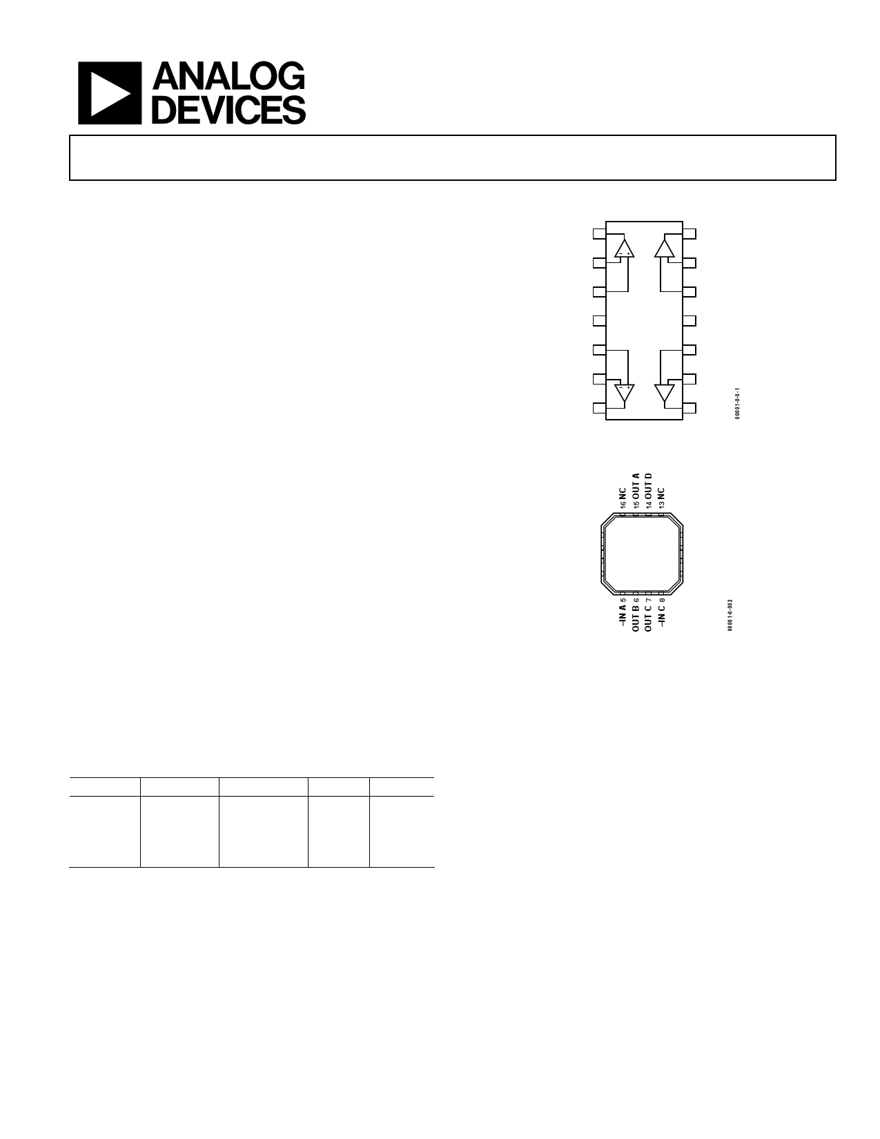
PIN CONFIGURATIONS
OUT A 1
–IN A 2
–+
14 OUT D
+–
13 –IN D
+IN A 3
12 +IN D
V+ 4 ADD8704 11 V–
+IN B 5
10 +IN C
–IN B 6
OUT B 7
–+
9 –IN C
+–
8 OUT C
Figure 1. 14-Lead TSSOP (RU Suffix)
–IN A 1
+IN A 2
V+ 3
+IN B 4
ADD8704
TOP VIEW
12 –IN D
11 +IN D
10 V–
9 +IN C
Figure 2. 16-Lead CSP (CP Suffix)
Rev. 0
Information furnished by Analog Devices is believed to be accurate and reliable.
However, no responsibility is assumed by Analog Devices for its use, nor for any
infringements of patents or other rights of third parties that may result from its use.
Specifications subject to change without notice. No license is granted by implication
or otherwise under any patent or patent rights of Analog Devices. Trademarks and
registered trademarks are the property of their respective owners.
One Technology Way, P.O. Box 9106, Norwood, MA 02062-9106, U.S.A.
Tel: 781.329.4700
www.analog.com
Fax: 781.326.8703 © 2003 Analog Devices, Inc. All rights reserved.
1 page 
ADD8704
ABSOLUTE MAXIMUM RATINGS
Table 3. ADD8704 Stress Ratings1
Parameter
Rating
Supply Voltage (VS)
Input Voltage
18 V
–0.5 V to VS + 0.5 V
Differential Input Voltage
VS
Storage Temperature Range
–65°C to +150°C
Operating Temperature Range
–40°C to +85°C
Junction Temperature Range
–65°C to +150°C
Lead Temperature Range
300°C
ESD Tolerance (HBM)
±1500 V
ESD Tolerance (MM)
175 V
Table 4. Package Characteristics
Package Type
θJA2 θJC Unit
14-Lead TSSOP (RU)
180 35 °C/W
16-Lead LFCSP (CP)
383 303 °C/W
1 Stresses above those listed under Absolute Maximum Ratings may cause
permanent damage to the device. This is a stress rating only; functional
operation of the device at these or any other conditions above those
indicated in the operational sections of this specification is not implied.
Exposure to absolute maximum rating conditions for extended periods may
affect device reliability.
2 θJA is specified for worst-case conditions, i.e., θJA is specified for devices
soldered onto a circuit board for surface-mount packages.
3 DAP is soldered down to PCB.
ESD CAUTION
ESD (electrostatic discharge) sensitive device. Electrostatic charges as high as 4000 V readily accumulate on the
human body and test equipment and can discharge without detection. Although this part features proprietary
ESD protection circuitry, permanent damage may occur on devices subjected to high energy electrostatic
discharges. Therefore, proper ESD precautions are recommended to avoid performance degradation or loss of
functionality.
Rev. 0 | Page 5 of 16
5 Page 
VDD = 16V
RL = 2kΩ
CL = 100pF
TIME (2µs/DIV)
Figure 33. Large Signal Transient Response
70
VS = 16V
60
MARKER SET @ 10kHz
MARKER READING = 25.7nV/ Hz
CHANNEL A, B, C
50
40
30
20
10
0
–10
0
5 10 15 20
FREQUENCY (Hz)
Figure 34. Voltage Noise Density vs. Frequency
25
ADD8704
70
VS = 16V
60
MARKER SET @ 10kHz
MARKER READING = 36.6nV/ Hz
CHANNEL D
50
40
30
20
10
0
–10
0
5 10 15 20
FREQUENCY (Hz)
Figure 35. Voltage Noise Density vs. Frequency
25
Rev. 0 | Page 11 of 16
11 Page | ||
| Páginas | Total 16 Páginas | |
| PDF Descargar | [ Datasheet ADD8704.PDF ] | |
Hoja de datos destacado
| Número de pieza | Descripción | Fabricantes |
| ADD8701 | 12-Channel Gamma Buffers with VCOM Buffer | Analog Devices |
| ADD8701 | 12-Channel Gamma Buffers with VCOM Buffer | Analog Devices |
| ADD8702 | 12-Channel Gamma Buffers | Analog Devices |
| ADD8704 | 16 V Quad Operational Amplifier | Analog Devices |
| Número de pieza | Descripción | Fabricantes |
| SLA6805M | High Voltage 3 phase Motor Driver IC. |
Sanken |
| SDC1742 | 12- and 14-Bit Hybrid Synchro / Resolver-to-Digital Converters. |
Analog Devices |
|
DataSheet.es es una pagina web que funciona como un repositorio de manuales o hoja de datos de muchos de los productos más populares, |
| DataSheet.es | 2020 | Privacy Policy | Contacto | Buscar |