|
|
PDF MBM30LV0128 Data sheet ( Hoja de datos )
| Número de pieza | MBM30LV0128 | |
| Descripción | 128 M (16 M X 8) BIT NAND-type | |
| Fabricantes | Fujitsu Media Devices | |
| Logotipo |  |
|
Hay una vista previa y un enlace de descarga de MBM30LV0128 (archivo pdf) en la parte inferior de esta página. Total 30 Páginas | ||
|
No Preview Available !
FUJITSU SEMICONDUCTOR
DATA SHEET
FLASH MEMORY
CMOS
DS05-20885-1E
128 M (16 M × 8) BIT NAND-type
MBM30LV0128
s DESCRIPTION
The MBM30LV0128 device is a single 3.3 V 16 M × 8 bit NAND flash memory organized as 528 byte × 32 pages
× 1024 blocks. Each 528 byte page contains 16 bytes of optionally selected spare area which may be used to
store ECC code (Specifications indicated are on condition that ECC system would be combined) . Program and
read data is transferred between the memory array and page register in 528 byte increments. A 528 byte page
can be programmed in 200 µs and an 16 K byte block can be erased in 2 ms under typical conditions. An internal
controller automates all programs and erases operations including the verification of data margins. Data within a
page can be read with a 50 ns cycle time per byte. The I/O pins are utilized for both address and data input/output
as well as command inputs. The MBM30LV0128 is an ideal solution for applications requiring mass non-volatile
storage such as solid state file storage, digital recording, image file memory for still cameras, and other uses
which require high density and non-volatile storage.
s PRODUCT LINE UP
Part No.
Operating Temperature
VCC
Read
Power Dissipation (Max.)
Erase / Program
TTL Standby
CMOS Standby
MBM30LV0128
−40 °C to +85 °C
+2.7 V to +3.6 V
72 mW
72 mW
3.6 mW
0.18 mW
1 page 
(Continued)
PIN Number
12
13, 36
1 to 5
10, 11
14, 15
20 to 24
25 to 28
33 to 35
38 to 40
45 to 48
Pin Name
VCC
VSS
Power Supply
Ground
N.C.
Non Connection
MBM30LV0128
Pin Functions
5
5 Page 
MBM30LV0128
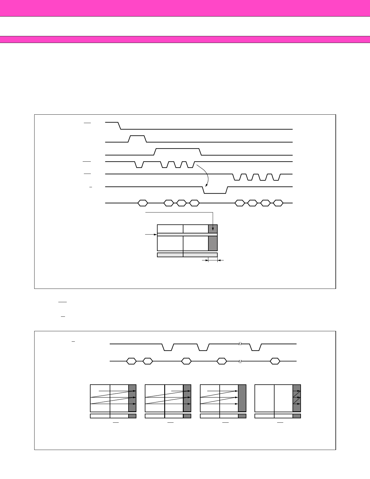
Read (3) : 50h
The Read (3) mode has identical timing to that of Read (1) and (2) . However, while Read (1) and (2) are used
to access the array, Read (3) is used to access the 16 byte spare area. When the 50h command is executed,
the pointer will be set to an address space between columns 512 and 527. The values of Y will complete the
address decoding. During this operation, only address bits A3 to A0 are used to determine the starting column
address; A7 to A4 are ignored. A23 to A9 are used to determine the starting row address.
CE
CLE
ALE
WE
RE
R/B
I/O0
to I/O7
Command 50h
Page (Row)
Address X
Starting Address
YXX
0 255 511 527
Data Output
Y (Column Address)
Figure 3 Read Mode (3) Operation
Sequential Read
Each RE pulse used to output data from the data register will cause the column address pointer to increment
by one. When the final column has been reached, the next page will be automatically loaded into the data register.
The R/B signal may be used to monitor the completion of the data transfer.
R/B
I/O0 to I/O7
0
00h/01h/50h Address Input Data
255 511 527 0
255 511 527 0
Data
255 511 527 0
Data
255 511 527
00h, SE = L
01h, SE = L
00h, SE = H
Figure 4 Sequential Read
50h, SE = L
11
11 Page | ||
| Páginas | Total 30 Páginas | |
| PDF Descargar | [ Datasheet MBM30LV0128.PDF ] | |
Hoja de datos destacado
| Número de pieza | Descripción | Fabricantes |
| MBM30LV0128 | 128 M (16 M X 8) BIT NAND-type | Fujitsu Media Devices |
| Número de pieza | Descripción | Fabricantes |
| SLA6805M | High Voltage 3 phase Motor Driver IC. |
Sanken |
| SDC1742 | 12- and 14-Bit Hybrid Synchro / Resolver-to-Digital Converters. |
Analog Devices |
|
DataSheet.es es una pagina web que funciona como un repositorio de manuales o hoja de datos de muchos de los productos más populares, |
| DataSheet.es | 2020 | Privacy Policy | Contacto | Buscar |
