|
|
PDF TFA3354 Data sheet ( Hoja de datos )
| Número de pieza | TFA3354 | |
| Descripción | Control and Monitoring IC for Electronic Ballasts | |
| Fabricantes | GSG | |
| Logotipo |  |
|
Hay una vista previa y un enlace de descarga de TFA3354 (archivo pdf) en la parte inferior de esta página. Total 12 Páginas | ||
|
No Preview Available !
GSG 勁力半導体
Gunter Semiconductor GmbH
TFA3354
EDITION 09/00
Control and Monitoring IC for
electronic ballast operating
fluorescent lamps. It triggers,
monitors and turns-off the RF
oscillation dependent on several
control- and guarding functions.
For inquiry please contact :
China
Tel: 0086-755-3200442
Hong Kong
Tel : 00852-26190748
e-mail
Fax: 0086-755-3355520
Fax: 00852-24948080
1 page 
Pin 3
TR
Trigger and Turn-off Output
This pin realizes three functions:
• Delivery of trigger pulses with a repetition instalment of 960 µs, a pulse width of 1 µs and a current flow of
600 mA with 10 Ω resistance.
• Monitoring of the control signals up to a frequency of 100 kHz and a minimum amplitude of 400 mV. The
oscillation detector gates trigger pulses, if a minimum three periode burst indicated during the trigger pulse
repetition rate.
• Attenuation of the oscillations by a turn-off transistor with a low saturation voltage.
Negative pulses may be applied at pin TR according the specification. Negative voltage peaks can cause an
increase of the current consumption. An external Schottky diode between TR and ground prevents this.
Pin 4
GND
Connection to ground
Pin 5
EI
Error Indication
At pin 5 it is possible to indicate different error values.
A static error signal greater than 3.75 V, which is supplied by a suitable network at pin 5 releases after one
second by means of an error enquiry cycle the storage of the error.
Furthermore the IC allows to supervise high-frequency oscillations.
An elaborate enquiry routine has been set up for secure and reliable acquisition of errors under consideration of
distortions. This routine consists of the valuation time of 840 µs with following evaluation time of 120 µs. These two
periods make the enquiry cycle repeating continuously, when no error signal is stored.
Signals with an amplitude > 3.75 V and a minimum duration of 1 µs are valuated as errors. If such events happen
at least 4 times within a time window of 840 µs, or a level > 3.75 V is statically applied, a counter starts to realize a
delay time of one second.
If those signals are detected again in the following valuation cycle, the error memory is setted.
This enquiry system saves that the RF-amplitude of the oscillating frequency is supervised, so that feed backs of
damaged lamps on the oscillation circuit would be detected.
The kind of lamp damage is depending on the type and sample of lamp. That is the reason for an adaptive
network for error detection, therefore the input EI is universal applicable.
Pin 6
LW
Input of Lamp Change
This input serves to detect a lamp change and cause a re-start with simultaneous reset of the error memory.
Input LW detects whether a lamp is connected, when a voltage > 4.25 V is applied.
A voltage < 3.25 V indicates a lamp as removed.
Is a lamp exchanged after a stored error, the error memory is reset and the trigger stop is activated.
The circuit is blocked without lamp. By removal a lamp the trigger gate is opened.
With a normal lamp change under operational conditions, triggers are continuously generated with lamp removed,
therefore, the circuit starts oscillation immediately by exchange of lamp.
The switching level for lamp change will be provided by a special circuitry.
For internal testing purposes at the input LW will be applied a special test level that decreases the internal time
response by factor 16.
This divider factor is active, if VLW is more than 2 V above VCC, but limited by max.15 V. Pay attention that the
voltage difference between VCC and VLW do not has to increase above 6 V also in case of supply voltage break
down.
Pin 7
S
Switching Output
The switching output enables the control of the preheat duration of the coiled filament by means of an additional
circuit to be selected by the customer.
The switching output is an open collector output which is low active for one second during the phase of start. It is
able to drive a maximum current of 1 mA at a typical saturation voltage of 200 mV.
4 09/00
TFA3354
5 Page 
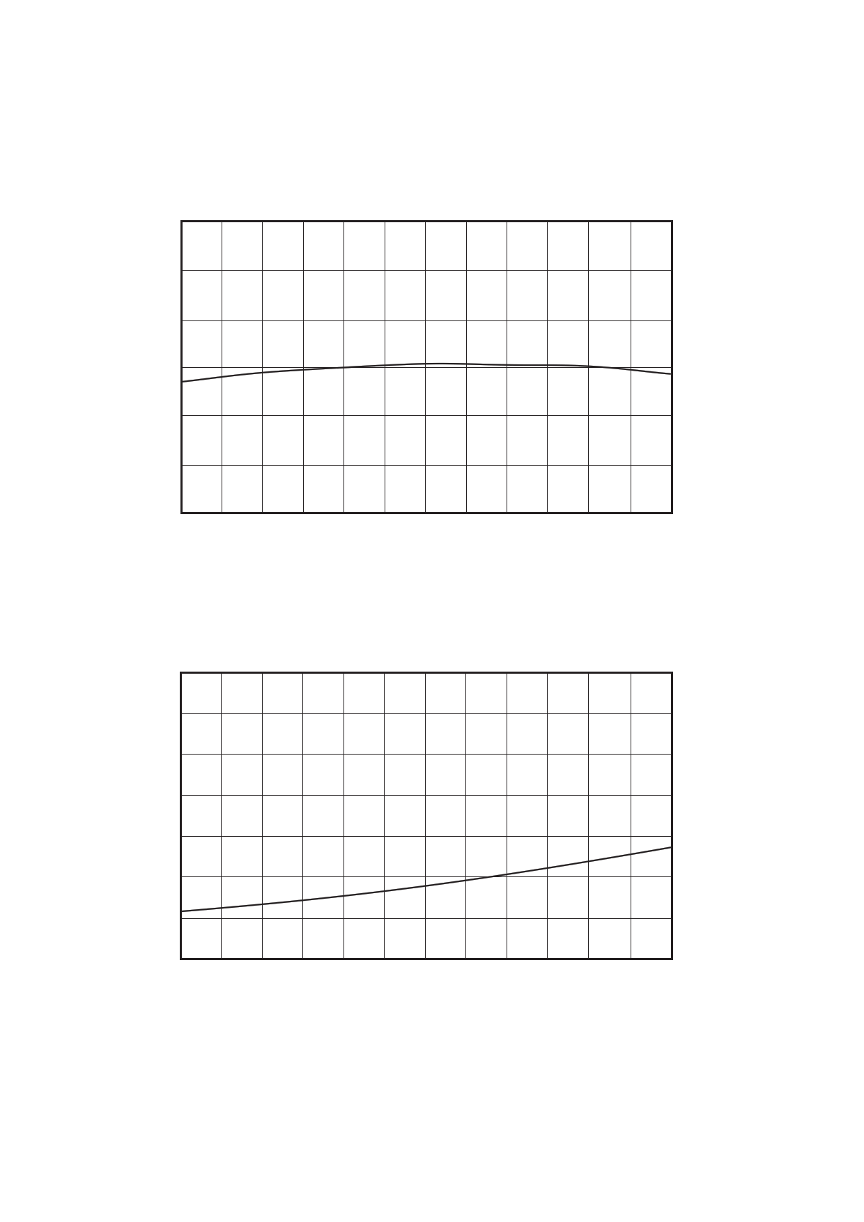
Static overload threshold
VCC = 10 V
3.90
3.80
3.75
3.70
3.65
3.60
-20 -10 0
10 20 30 40
50 60 70 Ta ( °C ) 100
Timer output saturation voltage at 1mA
VCC = 10 V
450
300
250
200
150
100
-20 -10 0
10 20 30 40
50 60 70 Ta ( °C ) 100
10 09/00
TFA3354
11 Page | ||
| Páginas | Total 12 Páginas | |
| PDF Descargar | [ Datasheet TFA3354.PDF ] | |
Hoja de datos destacado
| Número de pieza | Descripción | Fabricantes |
| TFA3354 | Control and Monitoring IC for Electronic Ballasts | GSG |
| Número de pieza | Descripción | Fabricantes |
| SLA6805M | High Voltage 3 phase Motor Driver IC. |
Sanken |
| SDC1742 | 12- and 14-Bit Hybrid Synchro / Resolver-to-Digital Converters. |
Analog Devices |
|
DataSheet.es es una pagina web que funciona como un repositorio de manuales o hoja de datos de muchos de los productos más populares, |
| DataSheet.es | 2020 | Privacy Policy | Contacto | Buscar |
