|
|
|
PDF MC74VHC1G00 Data sheet ( Hoja de datos )
| Número de pieza | MC74VHC1G00 | |
| Descripción | Single 2−Input NAND Gate | |
| Fabricantes | ON Semiconductor | |
| Logotipo | ||
Hay una vista previa y un enlace de descarga de MC74VHC1G00 (archivo pdf) en la parte inferior de esta página. Total 6 Páginas | ||
|
No Preview Available !
MC74VHC1G00
Single 2−Input NAND Gate
The MC74VHC1G00 is an advanced high speed CMOS 2−input
NAND gate fabricated with silicon gate CMOS technology.
The internal circuit is composed of multiple stages, including a
buffer output which provides high noise immunity and stable output.
The MC74VHC1G00 input structure provides protection when
voltages up to 7.0 V are applied, regardless of the supply voltage. This
allows the MC74VHC1G00 to be used to interface 5.0 V circuits to
3.0 V circuits.
Features
• High Speed: tPD = 3.0 ns (Typ) at VCC = 5.0 V
• Low Power Dissipation: ICC = 1 mA (Max) at TA = 25°C
• Power Down Protection Provided on Inputs
• Balanced Propagation Delays
• Pin and Function Compatible with Other Standard Logic Families
• Chip Complexity: FETs = 56
• Pb−Free Packages are Available
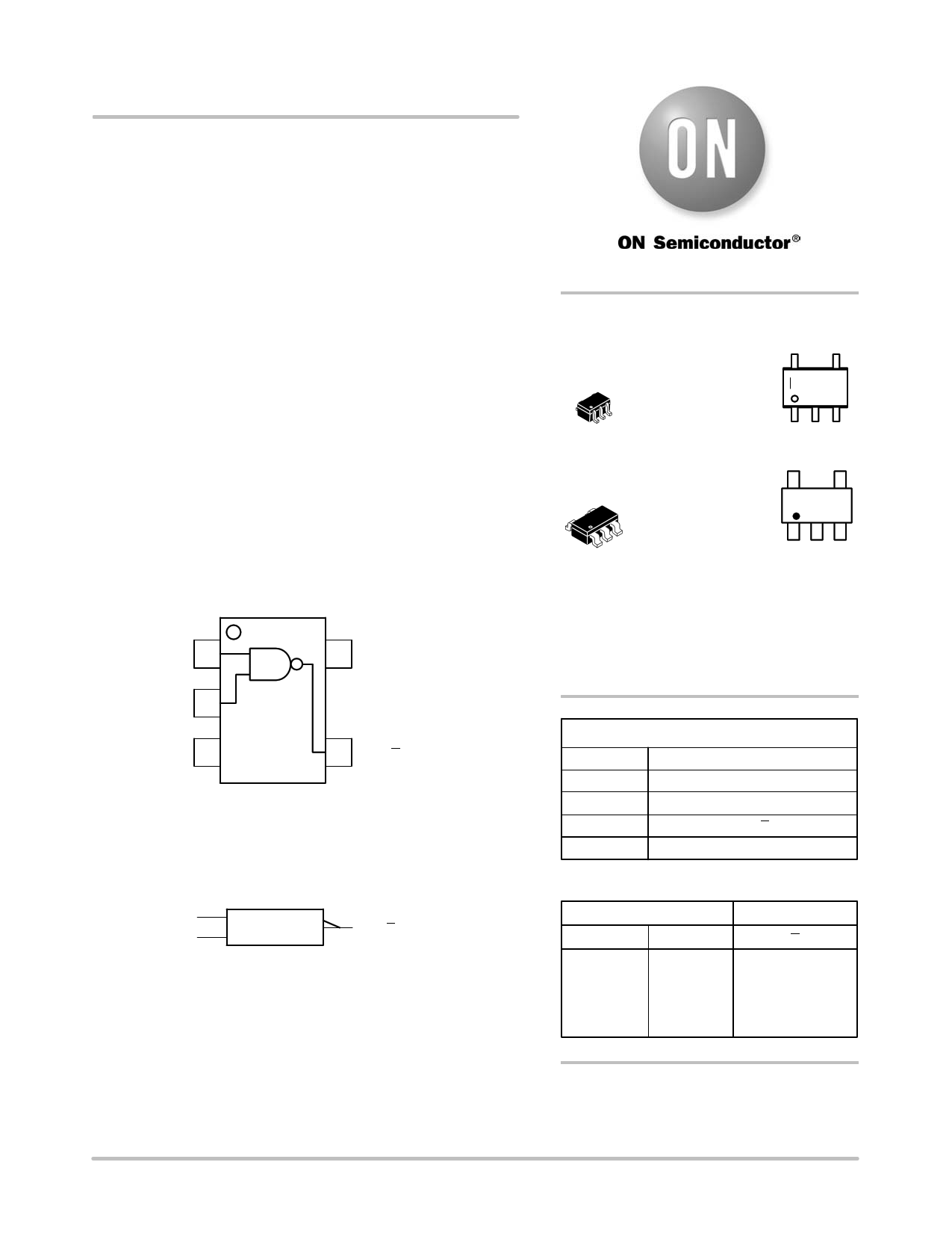
IN B 1
IN A 2
GND 3
5 VCC
4 OUT Y
Figure 1. Pinout (Top View)
IN A & OUT Y
IN B
Figure 2. Logic Symbol
http://onsemi.com
MARKING
DIAGRAMS
5
SC70−5/SC−88A/SOT−353
DF SUFFIX
CASE 419A
V1M G
G
1
1
SOT23−5/TSOP−5/SC59−5
DT SUFFIX
CASE 483
5
V1 M G
G
1
1
V1 = Device Code
M = Date Code*
G = Pb−Free Package
(Note: Microdot may be in either location)
*Date Code orientation and/or position may
vary depending upon manufacturing location.
PIN ASSIGNMENT
1 IN B
2 IN A
3 GND
4 OUT Y
5 VCC
FUNCTION TABLE
Inputs
Output
AB
LL
LH
HL
HH
Y
H
H
H
L
© Semiconductor Components Industries, LLC, 2007
January, 2007 − Rev. 18
ORDERING INFORMATION
See detailed ordering and shipping information in the package
dimensions section on page 4 of this data sheet.
1 Publication Order Number:
MC74VHC1G00/D
1 page 
MC74VHC1G00
PACKAGE DIMENSIONS
SC−88A/SOT−353/SC−70
DF SUFFIX
5 LEAD PACKAGE
CASE 419A−02
ISSUE J
A
G
54
S −B−
12
3
D 5 PL
0.2 (0.008) M B M
N
C
J
HK
NOTES:
1. DIMENSIONING AND TOLERANCING
PER ANSI Y14.5M, 1982.
2. CONTROLLING DIMENSION: INCH.
3. 419A−01 OBSOLETE. NEW STANDARD
419A−02.
4. DIMENSIONS A AND B DO NOT INCLUDE
MOLD FLASH, PROTRUSIONS, OR GATE
BURRS.
INCHES
DIM MIN MAX
A 0.071 0.087
B 0.045 0.053
C 0.031 0.043
D 0.004 0.012
G 0.026 BSC
H −−− 0.004
J 0.004 0.010
K 0.004 0.012
N 0.008 REF
S 0.079 0.087
MILLIMETERS
MIN MAX
1.80 2.20
1.15 1.35
0.80 1.10
0.10 0.30
0.65 BSC
−−− 0.10
0.10 0.25
0.10 0.30
0.20 REF
2.00 2.20
SOLDERING FOOTPRINT*
0.50
0.0197
0.65
0.025
0.40
0.0157
0.65
0.025
1.9
0.0748
ǒ ǓSCALE 20:1
mm
inches
*For additional information on our Pb−Free strategy and soldering
details, please download the ON Semiconductor Soldering and
Mounting Techniques Reference Manual, SOLDERRM/D.
http://onsemi.com
5
5 Page | ||
| Páginas | Total 6 Páginas | |
| PDF Descargar | [ Datasheet MC74VHC1G00.PDF ] | |
Hoja de datos destacado
| Número de pieza | Descripción | Fabricantes |
| MC74VHC1G00 | Single 2−Input NAND Gate | ON Semiconductor |
| MC74VHC1G01 | 2-Input NAND Gate with Open Drain Output | Leshan Radio Company |
| MC74VHC1G01 | 2-Input NAND Gate with Open Drain Output | ON Semiconductor |
| MC74VHC1G02 | 2-Input NOR Gate | Leshan Radio Company |
| Número de pieza | Descripción | Fabricantes |
| SLA6805M | High Voltage 3 phase Motor Driver IC. |
Sanken |
| SDC1742 | 12- and 14-Bit Hybrid Synchro / Resolver-to-Digital Converters. |
Analog Devices |
|
DataSheet.es es una pagina web que funciona como un repositorio de manuales o hoja de datos de muchos de los productos más populares, |
| DataSheet.es | 2020 | Privacy Policy | Contacto | Buscar |