|
|
PDF MC74VHC1GT32 Data sheet ( Hoja de datos )
| Número de pieza | MC74VHC1GT32 | |
| Descripción | 2-Input OR Gate/CMOS Logic Level Shifter | |
| Fabricantes | ON Semiconductor | |
| Logotipo | ||
Hay una vista previa y un enlace de descarga de MC74VHC1GT32 (archivo pdf) en la parte inferior de esta página. Total 8 Páginas | ||
|
No Preview Available !
MC74VHC1GT32
2-Input OR Gate/CMOS
Logic Level Shifter
The MC74VHC1GT32 is an advanced high speed CMOS 2–input OR
gate fabricated with silicon gate CMOS technology. It achieves high speed
operation similar to equivalent Bipolar Schottky TTL while maintaining
CMOS low power dissipation.
The internal circuit is composed of three stages, including a buffer
output which provides high noise immunity and stable output.
The device input is compatible with TTL–type input thresholds and the
output has a full 5 V CMOS level output swing. The input protection
circuitry on this device allows overvoltage tolerance on the input,
allowing the device to be used as a logic–level translator from 3.0 V
CMOS logic to 5.0 V CMOS Logic or from 1.8 V CMOS logic to 3.0 V
CMOS Logic while operating at the high–voltage power supply.
The MC74VHC1GT32 input structure provides protection when
voltages up to 7 V are applied, regardless of the supply voltage. This
allows the MC74VHC1GT32 to be used to interface 5 V circuits to 3 V
circuits. The output structures also provide protection when VCC = 0 V.
These input and output structures help prevent device destruction caused
by supply voltage – input/output voltage mismatch, battery backup, hot
insertion, etc.
• High Speed: tPD = 3.5 ns (Typ) at VCC = 5 V
• Low Power Dissipation: ICC = 2 µA (Max) at TA = 25°C
• TTL–Compatible Inputs: VIL = 0.8 V; VIH = 2.0 V
• CMOS–Compatible Outputs: VOH > 0.8 VCC; VOL < 0.1 VCC @Load
• Power Down Protection Provided on Inputs and Outputs
• Balanced Propagation Delays
• Pin and Function Compatible with Other Standard Logic Families
• Chip Complexity: FETs = 65; Equivalent Gates = 15
IN B 1
5 VCC
IN A 2
GND 3
4 OUT Y
Figure 1. Pinout (Top View)
http://onsemi.com
MARKING
DIAGRAMS
SC–88A / SOT–353/SC–70
DF SUFFIX
CASE 419A
VNd
Pin 1
d = Date Code
TSOP–5/SOT–23/SC–59
DT SUFFIX
CASE 483
VNd
Pin 1
d = Date Code
PIN ASSIGNMENT
1 IN B
2 IN A
3 GND
4 OUT Y
5 VCC
FUNCTION TABLE
Inputs
Output
AB
LL
LH
HL
HH
Y
L
H
H
H
IN A ≥ 1
IN B OUT Y
Figure 2. Logic Symbol
ORDERING INFORMATION
See detailed ordering and shipping information in the package
dimensions section on page 4 of this data sheet.
© Semiconductor Components Industries, LLC, 2001
November, 2001 – Rev. 4
1
Publication Order Number:
MC74VHC1GT32/D
1 page 
MC74VHC1GT32
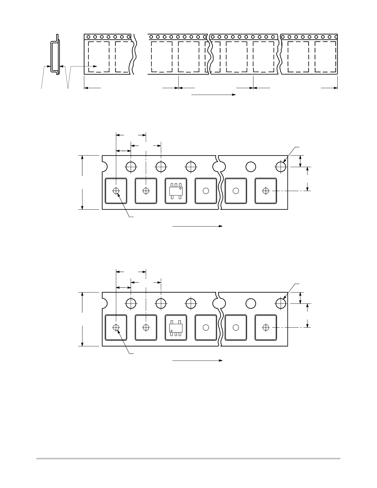
CAVITY TOP TAPE
TAPE
TAPE TRAILER
(Connected to Reel Hub)
NO COMPONENTS
160 mm MIN
COMPONENTS
DIRECTION OF FEED
Figure 6. Tape Ends for Finished Goods
TAPE DIMENSIONS mm
2.00
4.00
4.00
8.00 $0.30
TAPE LEADER
NO COMPONENTS
400 mm MIN
Ğ1.50 TYP
1.75
3.50 $0.50
Ğ1.00 MIN
1
DIRECTION OF FEED
Figure 7. SC–70–5/SC–88A/SOT–353 DFT1 Reel Configuration/Orientation
TAPE DIMENSIONS mm
2.00
4.00
4.00
8.00 $0.30
Ğ1.50 TYP
1.75
3.50 $0.50
Ğ1.00 MIN
1
DIRECTION OF FEED
Figure 8. SC–70/SC–88A/SOT–353 DFT2 and SOT23–5/TSOP–5/SC59–5 DTT1 Reel Configuration/Orientation
http://onsemi.com
5
5 Page | ||
| Páginas | Total 8 Páginas | |
| PDF Descargar | [ Datasheet MC74VHC1GT32.PDF ] | |
Hoja de datos destacado
| Número de pieza | Descripción | Fabricantes |
| MC74VHC1GT32 | 2-Input OR Gate/CMOS Logic Level Shifter | ON Semiconductor |
| Número de pieza | Descripción | Fabricantes |
| SLA6805M | High Voltage 3 phase Motor Driver IC. |
Sanken |
| SDC1742 | 12- and 14-Bit Hybrid Synchro / Resolver-to-Digital Converters. |
Analog Devices |
|
DataSheet.es es una pagina web que funciona como un repositorio de manuales o hoja de datos de muchos de los productos más populares, |
| DataSheet.es | 2020 | Privacy Policy | Contacto | Buscar |
