|
|
|
PDF ICS9248-64 Data sheet ( Hoja de datos )
| Número de pieza | ICS9248-64 | |
| Descripción | Frequency Generator & Integrated Buffers | |
| Fabricantes | Integrated Circuit Systems | |
| Logotipo | ||
Hay una vista previa y un enlace de descarga de ICS9248-64 (archivo pdf) en la parte inferior de esta página. Total 15 Páginas | ||
|
No Preview Available !
Integrated
Circuit
Systems, Inc.
ICS9248-64
AMD-K7TM System Clock Chip
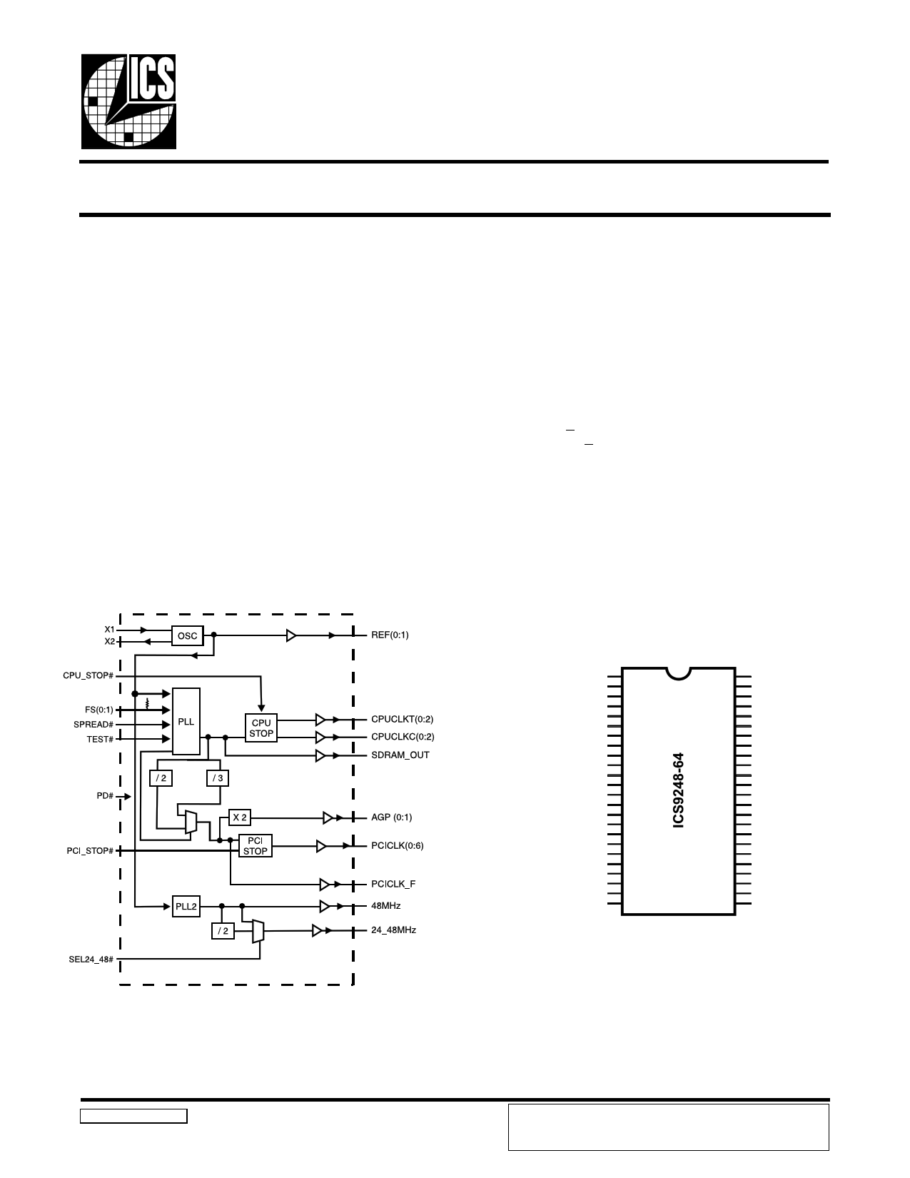
General Description
The ICS9248-64 is a main clock synthesizer chip for AMD-
K7 based systems. This provides all clocks required for such
a system when used with a Zero Delay Buffer Chip such as
the ICS9179-06.
Spread Spectrum may be enabled by driving the SPREAD#
pin active. Spread spectrum typically reduces system EMI by
8dB to 10dB. This simplifies EMI qualification without
resorting to board design iterations or costly shielding. The
ICS9248-64 employs a proprietary closed loop design, which
tightly controls the percentage of spreading over process and
temperature variations.
Features
• Generates the following system clocks:
- 3 differential pair open drain CPU clocks
(1.5V external
pull-up; up to 133MHz).
- 8 PCI including 1 free running (3.3V) @33.3MHz.
- 2 AGP(3.3V) up to 66.6MHz.
- 2 REF(3.3V)@14.318MHz
- 1 48MHz(3.3V)
- 24 / 48MHz(3.3V)
• Skew characteristics:
- CPU -CPU<250ps
- CPUt - CPUc <200ps (differential pair)
- PCI – PCI: <500ps
- CPU – SDRAM_OUT: < 250ps
- CPU – AGP <500ps
Block Diagram
• Efficient Power Management through PD#, PCI_STOP#
and CPU_STOP#.
• Spread Spectrum option for EMI reduction
(-1.0% down spread).
• Uses external 14.318 MHz crystal
Pin Configuration
*FS0/REF0
*FS1/REF1
GNDREF
X1
X2
GNDPCI
PCICLK_F
PCICLK0
VDDPCI
PCICLK1
PCICLK2
GNDPCI
PCICLK3
PCICLK4
VDDPCI
PCICLK5
PCICLK6
VDDAGP
AGP0
AGP1
GNDAGP
VDD48
48MHz
SEL24_48#/24-48MHz
1
2
3
4
5
6
7
8
9
10
11
12
13
14
15
16
17
18
19
20
21
22
23
24
48 VDDREF
47 GNDSD
46 SDRAM_OUT
45 VDDSD
44 RESERVED
43 CPUCLKC2
42 CPUCLKT2
41 GNDCPU
40 CUCLKC1
39 CPUCLKT1
38 GND
37 CPUCLKC0
36 CPUCLKT0
35 RESERVED
34 VDD
33 GND
32 PCI_STOP#
31 CPU_STOP#
30 PD#
29 SPREAD#
28 TEST#
{27
26
SDATA
SCLK
I2C
25 GND48
48-Pin SSOP
* Internal 120K pullup resistor on indicated inputs
9248-64 Rev C 03/19/01
AMD-K is a trademark of Advanced Micro Devices.
ICS reserves the right to make changes in the device data identified in
this publication without further notice. ICS advises its customers to
obtain the latest version of all device data to verify that any
information being relied upon by the customer is current and accurate.
1 page 
ICS9248-64
Byte 4: Clock Control Register
BIT PIN# PWD
DESCRIPTION
7 1 1 REF0 enable
6 24 1 24MHz/48MHz enable
5 23 1 48MHz enable
4 20 1 AGP1 enable
3 19 1 AGP0 enable
CPUCLK2 enable (both of
2 42, 43 1 differential pair, True" and
"Complimentary"
CPUCLK1 enable (both of
1 39, 40 1 differential pair, True" and
"Complimentary"
CPUCLK0 enable (both of
0 36, 37 1 differential pair, True" and
"Complimentary"
Notes: A value of '1'b is enable, '0'b is disable
Byte 5: PCI Clock Control Register
BIT PIN# PWD
DESCRIPTION
7 2 1 REF1 enable
6 17 1 PCICLK6 enable
5 16 1 PCICLK5 enable
4 14 1 PCICLK4 enable
3 13 1 PCICLK3 enable
2 11 1 PCICLK2 enable
1 10 1 PCICLK1 enable
0 8 1 PCICLK0 enable
Notes: A value of '1'b is enable, '0'b is disable
Byte 6: SDRAM Clock & Generator Mode Control Register
Bit
Description
PWD
7 Spread Spectrum enable down spread
1
Bit
654
CPU
PCI Spread Percentage
111 100
33.3 1% Down Spread
110 120
30 1% Down Spread
6:4
101
100
133
90
33.3 1% Down Spread
30 -0.5%Down Spread
011 TCLK/2 TCLK/6 1% Down Spread
1
010 66
33 -0.5%Down Spread
001 50
25 1% Down Spread
000 HI-Z
HI-Z 1% Down Spread
2:3 (Reserved)
1
1 I2C enable
1
0 SDRAM_OUT Enable
1
Notes: A value of '1'b is enable, '0'b is disable
5
5 Page 
ICS9248-64
Shared Pin Operation -
Input/Output Pins
The I/O pins designated by (input/output) on the ICS9248-
64 serve as dual signal functions to the device. During initial
power-up, they act as input pins. The logic level (voltage)
that is present on these pins at this time is read and stored
into a 5-bit internal data latch. At the end of Power-On reset,
(see AC characteristics for timing values), the device changes
the mode of operations for these pins to an output function.
In this mode the pins produce the specified buffered clocks
to external loads.
To program (load) the internal configuration register for these
pins, a resistor is connected to either the VDD (logic 1) power
supply or the GND (logic 0) voltage potential. A 10 Kilohm
(10K) resistor is used to provide both the solid CMOS
programming voltage needed during the power-up
programming period and to provide an insignificant load on
the output clock during the subsequent operating period.
Figure 1 shows a means of implementing this function when
a switch or 2 pin header is used. With no jumper is installed
the pin will be pulled high. With the jumper in place the pin
will be pulled low. If programmability is not necessary, than
only a single resistor is necessary. The programming resistors
should be located close to the series termination resistor to
minimize the current loop area. It is more important to locate
the series termination resistor close to the driver than the
programming resistor.
Programming
Header
Via to Gnd
Via to
VDD
2K W
Device
Pad
8.2K W
Clock trace to load
Series Term. Res.
Fig. 1
11
11 Page | ||
| Páginas | Total 15 Páginas | |
| PDF Descargar | [ Datasheet ICS9248-64.PDF ] | |
Hoja de datos destacado
| Número de pieza | Descripción | Fabricantes |
| ICS9248-61 | Frequency Generator & Integrated Buffers | Integrated Circuit Systems |
| ICS9248-64 | Frequency Generator & Integrated Buffers | Integrated Circuit Systems |
| ICS9248-65 | Frequency Generator & Integrated Buffers | Integrated Circuit Systems |
| ICS9248-66 | Frequency Generator & Integrated Buffers | Integrated Circuit Systems |
| Número de pieza | Descripción | Fabricantes |
| SLA6805M | High Voltage 3 phase Motor Driver IC. |
Sanken |
| SDC1742 | 12- and 14-Bit Hybrid Synchro / Resolver-to-Digital Converters. |
Analog Devices |
|
DataSheet.es es una pagina web que funciona como un repositorio de manuales o hoja de datos de muchos de los productos más populares, |
| DataSheet.es | 2020 | Privacy Policy | Contacto | Buscar |