|
|
|
PDF ICS9248-143 Data sheet ( Hoja de datos )
| Número de pieza | ICS9248-143 | |
| Descripción | Frequency Generator & Integrated Buffers | |
| Fabricantes | Integrated Circuit Systems | |
| Logotipo | ||
Hay una vista previa y un enlace de descarga de ICS9248-143 (archivo pdf) en la parte inferior de esta página. Total 16 Páginas | ||
|
No Preview Available !
Integrated
Circuit
Systems, Inc.
ICS9248 - 143
Frequency Generator & Integrated Buffers for PENTIUM II/IIITM & K6
RecommendedApplication:
440BX, MX, VIAApollo Pro 133,Apollo Pro Media
or MVP4 style chip set, for Note book applications.
Output Features:
4 - CPUs @ 2.5V/3.3V
including 1 free running CPUCLK_F
9 - SDRAM @ 3.3V
7 - PCI @ 3.3V, including 1 free running PCICLK_F
1 - PCI Early @ 3.3V
1 - 48MHz, @ 3.3V fixed.
1 - 24/48MHz @ 3.3V
2 - REF @3.3V, 14.318MHz.
Features:
Up to 137MHz frequency support
97MHz to support high-end AMD processor.
Support power management: CLK, PCI, stop and Power
down Mode from I2C programming.
Spread spectrum for EMI control
(±.25% & 0 to -0.5% down spread).
Uses external 14.318MHz crystal
FS pins for frequency select
Key Specifications:
CPU Output Jitter @ 2.5V: <300ps
CPU Output Jitter @ 3.3V: <250ps
PCI Output Jitter @ 3.3V: <250ps
CPU Output Skew @ 2.5V: <175ps
CPU Output Skew @ 3.3V: <175ps
PCI Output Skew @ 3.3V: <500ps
PCI Early to PCI Skew @ 3.3V: typ = 3ns
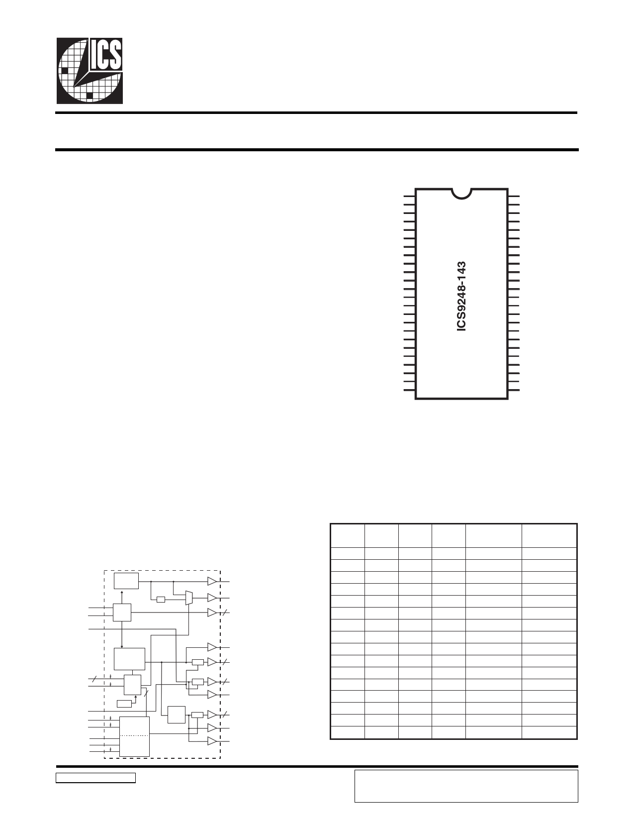
Block Diagram
X1
X2
BUFFER IN
FS(0:3) 4
SEL24_48#
CLK_STOP#
PCI_STOP#
CPU2.5_3.3#
SDATA
SCLK
PD#
PLL2
XTAL
OSC
/2
PLL1
Spread
Spectrum
LATCH
POR
4
Control
Logic
Config.
Reg.
STOP
STOP
PCI
CLOCK
DIVDER
STOP
48MHz
24_48MHz
2 REF[1:0]
CPUCLK_F
3 CPUCLK [2:0]
8 SDRAM [7:0]
SDRAM_F
PCICLK [5:0]
6
PCICLK_F
PCICLK_E
9248-143 Rev C 7/26/00
Pin Configuration
VDDREF
*SPREAD/REF0
GNDREF
X1
X2
VDDPCI
*CPU2.5_3.3#/PCICLK_F
*FS3/PCICLK0
GNDPCI
*SEL24_48#/PCICLK1
*SELPCIE_6#/PCICLK2
PCICLK3
PCICLK4
VDDPCI
BUFFER IN
GNDPCI
PCICLK5
PCICLK6/PCICLK_E
VDDCOR
PCI_STOP#
*PD#
GND48
SDATA
SCLK
1
2
3
4
5
6
7
8
9
10
11
12
13
14
15
16
17
18
19
20
21
22
23
24
48 REF1/FS2*
47 VDDLCPU
46 CPUCLK_F
45 CPUCLK0
44 GNDLCPU
43 CPUCLK1
42 CPUCLK2
41 CLK_STOP#
40 GNDSDR
39 SDRAM_F
38 SDRAM0
37 SDRAM1
36 VDDSDR
35 SDRAM2
34 SDRAM3
33 GNDSDR
32 SDRAM4
31 SDRAM5
30 VDDSDR
29 SDRAM6
28 SDRAM7
27 VDD48
26 48MHz/FS0*
25 24_48MHz/FS1*
48-Pin SSOP and TSSOP
* Internal Pull-up Resistor of 120K to VDD
Functionality
FS3 FS2 FS1 FS0
0000
000 1
00 10
00 11
0 100
0 10 1
0 110
0 111
10 0 0
100 1
10
10
10 11
1 10 0
110 1
1 1 10
1111
CPU
(MHz)
66.67
100.00
100.30
133.33
105.00
133.37
137.00
75.00
100.00
95.00
97.00
133.33
90.00
96.22
66.82
91.50
PCI
(MHz)
33.33
33.33
33.43
33.33
35.00
33.34
34.25
37.50
33.33
31.67
32.33
33.33
30.00
32.07
33.41
30.50
Pentium is a trademark of Intel Corporation
I2C is a trademark of Philips Corporation
ICS reserves the right to make changes in the device data identified in
this publication without further notice. ICS advises its customers to
obtain the latest version of all device data to verify that any
information being relied upon by the customer is current and accurate.
1 page 
ICS9248 - 143
Byte 4: Reserved Active/Inactive Register (1 = enable, 0 = disable)
Bit
Bit 7
Bit 6
Bit 5
Bit 4
Bit 3
Bit 2
Bit 1
Bit 0
Pin #
-
-
-
-
-
-
-
-
PWD
1
1
X
1
X
1
X
1
Description
(Reserved)
(Reserved)
(SEL24_48)#
(Reserved)
Latched FS1#
(Reserved)
Latched FS3#
(Reserved)
Byte 5: Peripheral Active/Inactive Register (1 = enable, 0 = disable)
Bit
Bit 7
Bit 6
Bit 5
Bit 4
Bit 3
Bit 2
Bit 1
Bit 0
Pin #
34
35
37
38
26
25
48
2
PWD
1
1
1
1
1
1
1
1
Description
SDRAM3 (Act/Inact)
SDRAM2 (Act/Inact)
SDRAM1 (Act/Inact)
SDRAM0 (Act/Inact)
48MHz (Act/Inact)
24MHz (Act/Inact)
REF1 (Act/Inact)
REF0 (Act/Inact)
Notes:
1. Inactive means outputs are held LOW and are disabled from switching.
2. Latched Frequency Selects (FS#) will be inverted logic load of the input frequency select pin conditions.
5
5 Page 
ICS9248 - 143
Shared Pin Operation -
Input/Output Pins
The I/O pins designated by (input/output) on the ICS9248-
143 serve as dual signal functions to the device. During initial
power-up, they act as input pins. The logic level (voltage)
that is present on these pins at this time is read and stored
into a 5-bit internal data latch. At the end of Power-On reset,
(see AC characteristics for timing values), the device changes
the mode of operations for these pins to an output function.
In this mode the pins produce the specified buffered clocks
to external loads.
To program (load) the internal configuration register for these
pins, a resistor is connected to either the VDD (logic 1) power
supply or the GND (logic 0) voltage potential. A 10 Kilohm
(10K) resistor is used to provide both the solid CMOS
programming voltage needed during the power-up
programming period and to provide an insignificant load on
the output clock during the subsequent operating period.
Figure 1 shows a means of implementing this function when
a switch or 2 pin header is used. With no jumper is installed
the pin will be pulled high. With the jumper in place the pin
will be pulled low. If programmability is not necessary, than
only a single resistor is necessary. The programming resistors
should be located close to the series termination resistor to
minimize the current loop area. It is more important to locate
the series termination resistor close to the driver than the
programming resistor.
Programming
Header
Via to Gnd
Via to
VDD
2K W
Device
Pad
8.2K W
Clock trace to load
Series Term. Res.
Fig. 1
11
11 Page | ||
| Páginas | Total 16 Páginas | |
| PDF Descargar | [ Datasheet ICS9248-143.PDF ] | |
Hoja de datos destacado
| Número de pieza | Descripción | Fabricantes |
| ICS9248-141 | Frequency Generator & Integrated Buffers | Integrated Circuit Systems |
| ICS9248-143 | Frequency Generator & Integrated Buffers | Integrated Circuit Systems |
| ICS9248-146 | Frequency Generator & Integrated Buffers | Integrated Circuit Systems |
| Número de pieza | Descripción | Fabricantes |
| SLA6805M | High Voltage 3 phase Motor Driver IC. |
Sanken |
| SDC1742 | 12- and 14-Bit Hybrid Synchro / Resolver-to-Digital Converters. |
Analog Devices |
|
DataSheet.es es una pagina web que funciona como un repositorio de manuales o hoja de datos de muchos de los productos más populares, |
| DataSheet.es | 2020 | Privacy Policy | Contacto | Buscar |