|
|
|
PDF HCPL-7710 Data sheet ( Hoja de datos )
| Número de pieza | HCPL-7710 | |
| Descripción | 40 ns Propagation Delay / CMOS Optocoupler | |
| Fabricantes | Hewlett-Packard | |
| Logotipo | ||
Hay una vista previa y un enlace de descarga de HCPL-7710 (archivo pdf) en la parte inferior de esta página. Total 17 Páginas | ||
|
No Preview Available !
Agilent HCPL-7710, HCPL-0710
40 ns Propagation Delay,
CMOS Optocoupler
Data Sheet
Description
Available in either an 8-pin DIP or
SO-8 package style respectively,
the HCPL-7710 or HCPL-0710
optocouplers utilize the latest
CMOS IC technology to achieve
outstanding performance with
very low power consumption. The
HCPL-x710 require only two
bypass capacitors for complete
CMOS compatibility.
Basic building blocks of the
HCPL-x710 are a CMOS LED
driver IC, a high speed LED and a
CMOS detector IC. A CMOS logic
input signal controls the LED
driver IC which supplies current
to the LED. The detector IC
incorporates an integrated
photodiode, a high-speed
transimpedance amplifier, and a
voltage comparator with an
output driver.
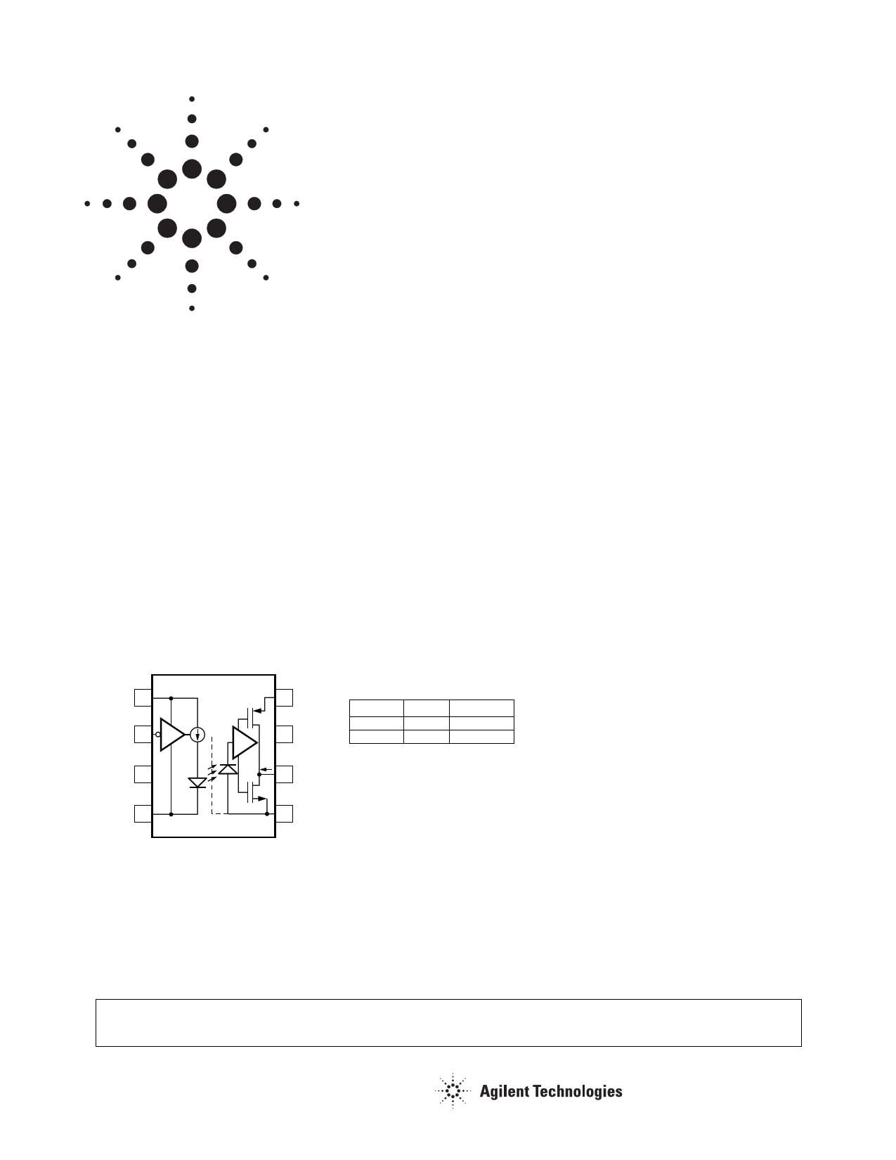
Functional Diagram
**VDD1 1
VI 2
*3
GND1 4
LED1
SHIELD
8 VDD2**
7 NC*
IO
6 VO
TRUTH TABLE
(POSITIVE LOGIC)
VI, INPUT
H
L
LED1
OFF
ON
VO, OUTPUT
H
L
5 GND2
Features
• +5 V CMOS compatibility
• 8 ns maximum pulse width
distortion
• 20 ns maximum prop. delay skew
• High speed: 12 Mbd
• 40 ns maximum prop. delay
• 10 kV/µs minimum common mode
rejection
• -40°C to 100°C temperature range
• Safety and regulatory approvals
UL Recognized
3750 V rms for 1 min. per
UL 1577
CSA Component Acceptance
Notice #5
IEC/EN/DIN EN 60747-5-2
– VIORM = 630 Vpeak for
HCPL-7710 Option 060
– VIORM = 560 Vpeak for
HCPL-0710 Option 060
Applications
• Digital fieldbus isolation:
DeviceNet, SDS, Profibus
• AC plasma display panel level
shifting
• Multiplexed data transmission
• Computer peripheral interface
• Microprocessor system interface
* Pin 3 is the anode of the internal LED and must be left unconnected for guaranteed data sheet
performance. Pin 7 is not connected internally.
** A 0.1 µF bypass capacitor must be connected between pins 1 and 4, and 5 and 8.
CAUTION: It is advised that normal static precautions be taken in handling and assembly of this
component to prevent damage and/or degradation which may be induced by ESD.
1 page 
IEC/EN/DIN EN 60747-5-2 Insulation Related Characteristics (Option 060)
Description
Installation classification per DIN VDE 0110/1.89, Table 1
for rated mains voltage ≤150 V rms
for rated mains voltage ≤300 V rms
for rated mains voltage ≤450 V rms
Climatic Classification
Pollution Degree (DIN VDE 0110/1.89)
Maximum Working Insulation Voltage
Input to Output Test Voltage, Method b†
VIORM x 1.875 = VPR, 100% Production
Test with tm = 1 sec, Partial Discharge < 5 pC
Input to Output Test Voltage, Method a†
VIORM x 1.5 = VPR, Type and Sample Test,
tm = 60 sec, Partial Discharge < 5 pC
Highest Allowable Overvoltage†
(Transient Overvoltage, tini = 10 sec)
Safety Limiting Values
(Maximum values allowed in the event of a failure,
also see Thermal Derating curve, Figure 11.)
Case Temperature
Input Current
Output Power
Insulation Resistance at TS, V10 = 500 V
Symbol
VIORM
VPR
VPR
VIOTM
TS
IS,INPUT
PS,OUTPUT
RIO
HCPL-7710
Option 060
I-IV
I-IV
I-III
55/100/21
2
630
1181
945
6000
175
230
600
≥109
HCPL-0710
Option 060
I-IV
I-III
55/100/21
2
560
1050
Units
V peak
V peak
840 V peak
4000 V peak
150 °C
150 mA
600 mW
≥109
Ω
†Refer to the front of the optocoupler section of the Isolation and Control Component Designer’s Catalog, under Product Safety Regulations section
IEC/EN/DIN EN 60747-5-2, for a detailed description.
Note: These optocouplers are suitable for “safe electrical isolation” only within the safety limit data. Maintenance of the safety data shall be ensured
by means of protective circuits.
Note: The surface mount classification is Class A in accordance with CECC 00802.
Absolute Maximum Ratings
Parameter
Storage Temperature
Ambient Operating Temperature
Supply Voltages
Input Voltage
Output Voltage
Input Current
Average Output Current
Lead Solder Temperature
Solder Reflow Temperature Profile
Symbol Min. Max.
Units
TS
–55 125
°C
TA –40 +100 °C
VDD1, VDD2
0
6.0
Volts
VI
–0.5
VDD1 +0.5
Volts
VO
–0.5
VDD2 +0.5
Volts
II
–10 +10
mA
IO 10 mA
260°C for 10 sec., 1.6 mm below seating plane
See Solder Reflow Temperature Profile Section
Figure
Recommended Operating Conditions
Parameter
Ambient Operating Temperature
Supply Voltages
Logic High Input Voltage
Logic Low Input Voltage
Input Signal Rise and Fall Times
Symbol
TA
VDD1, VDD2
VIH
VIL
tr, tf
Min.
–40
4.5
2.0
0.0
Max.
+100
5.5
VDD1
0.8
1.0
Units
°C
V
V
V
ms
Figure
1, 2
5
5 Page 
Digital Field Bus Communication
Networks
To date, despite its many draw-
backs, the 4 - 20 mA analog
current loop has been the most
widely accepted standard for
implementing process control
systems. In today’s manufacturing
environment, however, automated
systems are expected to help
manage the process, not merely
monitor it. With the advent of
digital field bus communication
networks such as DeviceNet,
PROFIBUS, and Smart
Distributed Systems (SDS), gone
are the days of constrained
information. Controllers can now
receive multiple readings from
field devices (sensors, actuators,
etc.) in addition to diagnostic
information.
The physical model for each of
these digital field bus communica-
tion networks is very similar as
shown in Figure 17. Each includes
one or more buses, an interface
unit, optical isolation, transceiver,
and sensing and/or actuating
devices.
CONTROLLER
BUS
INTERFACE
OPTICAL
ISOLATION
TRANSCEIVER
FIELD BUS
TRANSCEIVER
OPTICAL
ISOLATION
BUS
INTERFACE
TRANSCEIVER
OPTICAL
ISOLATION
BUS
INTERFACE
TRANSCEIVER
OPTICAL
ISOLATION
BUS
INTERFACE
TRANSCEIVER
OPTICAL
ISOLATION
BUS
INTERFACE
DEVICE
CONFIGURATION
MOTOR
STARTER
Figure 17. Typical field bus communication physical model.
XXXXXX
YYY
MOTOR
CONTROLLER
SENSOR
Optical Isolation for Field Bus
Networks
To recognize the full benefits of
these networks, each recommends
providing galvanic isolation using
Agilent optocouplers. Since
network communication is bi-
directional (involving receiving
data from and transmitting data
onto the network), two Agilent
optocouplers are needed. By
providing galvanic isolation, data
integrity is retained via noise
reduction and the elimination of
false signals. In addition, the
network receives maximum
protection from power system
faults and ground loops.
Within an isolated node, such as
the DeviceNet Node shown in
Figure 18, some of the node’s
components are referenced to a
ground other than V- of the
network. These components could
include such things as devices
with serial ports, parallel ports,
RS232 and RS485 type ports. As
shown in Figure 18, power from
the network is used only for the
transceiver and input (network)
side of the optocouplers.
Isolation of nodes connected to
any of the three types of digital
field bus networks is best
achieved by using the HCPL-x710
optocouplers. For each network,
the HCPL-x710 satisify the critical
propagation delay and pulse
width distortion requirements
over the temperature range of 0°C
to +85°C, and power supply
voltage range of 4.5 V to 5.5 V.
11
11 Page | ||
| Páginas | Total 17 Páginas | |
| PDF Descargar | [ Datasheet HCPL-7710.PDF ] | |
Hoja de datos destacado
| Número de pieza | Descripción | Fabricantes |
| HCPL-7710 | 40 ns Propagation Delay / CMOS Optocoupler | Hewlett-Packard |
| HCPL-7710 | 40 ns Propagation Delay / CMOS Optocoupler | Avago |
| Número de pieza | Descripción | Fabricantes |
| SLA6805M | High Voltage 3 phase Motor Driver IC. |
Sanken |
| SDC1742 | 12- and 14-Bit Hybrid Synchro / Resolver-to-Digital Converters. |
Analog Devices |
|
DataSheet.es es una pagina web que funciona como un repositorio de manuales o hoja de datos de muchos de los productos más populares, |
| DataSheet.es | 2020 | Privacy Policy | Contacto | Buscar |