|
|
PDF IC41C1665 Data sheet ( Hoja de datos )
| Número de pieza | IC41C1665 | |
| Descripción | 64K x16 bit Dynamic RAM with Fast Page Mode | |
| Fabricantes | ICSI | |
| Logotipo |  |
|
Hay una vista previa y un enlace de descarga de IC41C1665 (archivo pdf) en la parte inferior de esta página. Total 19 Páginas | ||
|
No Preview Available !
IC41C1665
IC41LV1665
Document Title
64K x16 bit Dynamic RAM with Fast Page Mode
Revision History
Revision No
0A
History
Initial Draft
Draft Date
Remark
October 17,2001
The attached datasheets are provided by ICSI. Integrated Circuit Solution Inc reserve the right to change the specifications and
products. ICSI will answer to your questions about device. If you have any questions, please contact the ICSI offices.
Integrated Circuit Solution Inc.
DR031-0A 10/17/2001
1
1 page 
IC41C1665
IC41LV1665
FUNCTIONAL DESCRIPTION
The IC41C1665 and the IC41LV1665 are CMOS DRAMs
optimized for high-speed bandwidth, low-power applications.
During READ or WRITE cycles, each bit is uniquely
addressed through the 16 address bits. These are entered
nine bits (A0-A7) at a time. The row address is latched by the
Row Address Strobe (RAS). The column address is latched
by the Column Address Strobe (CAS). RAS is used to latch
the first eight bits and CAS is used to latch the latter eight
bits.
The IC41C1665 and the IC41LV1665 have two CAS controls,
LCAS and UCAS. The LCAS and UCAS inputs internally
generate a CAS signal functioning in an identical manner to
the single CAS input on the other 64K x 16 DRAMs. The key
difference is that each CAS controls its corresponding I/O
tristate logic (in conjunction with OE and WE and RAS).
LCAS controls I/O0 - I/O7 and UCAS controls I/O8 - I/O15.
The IC41C1665/IC41LV1665 CAS function is determined by
the first CAS (LCAS or UCAS) transitioning LOW and the last
transitioning back HIGH. The two CAS controls give the
IC41C1665 both BYTE READ and BYTE WRITE cycle
capabilities.
Write Cycle
A write cycle is initiated by the falling edge of CAS and WE,
whichever occurs last. The input data must be valid at or
before the falling edge of CAS or WE, whichever occurs last.
Refresh Cycle
To retain data, 256 refresh cycles are required in each
4 ms period. There are two ways to refresh the memory:
1. By clocking each of the 256 row addresses (A0 through
A7) with RAS at least once every 4 ms. Any read, write,
read-modify-write or RAS-only cycle refreshes the ad-
dressed row.
2. Using a CAS-before-RAS refresh cycle. CAS-before-RAS
refresh is activated by the falling edge of RAS, while
holding CAS LOW. In CAS-before-RAS refresh cycle, an
internal 8-bit counter provides the row addresses and the
external address inputs are ignored.
CAS-before-RAS is a refresh-only mode and no data access
or device selection is allowed. Thus, the output remains in
the High-Z state during the cycle.
Memory Cycle
A memory cycle is initiated by bringing RAS LOW and it is
terminated by returning both RAS and CAS HIGH. To
ensure proper device operation and data integrity any
memory cycle, once initiated, must not be ended or aborted
before the minimum tRAS time has expired. A new cycle must
not be initiated until the minimum precharge time tRP, tCP has
elapsed.
Power-On
After application of the VCC supply, an initial pause of
200 µs is required followed by a minimum of eight initialization
cycles (any combination of cycles containing a RAS signal).
During power-on, it is recommended that RAS track with VCC
or be held at a valid VIH to avoid current surges.
Read Cycle
A read cycle is initiated by the falling edge of CAS or OE,
whichever occurs last, while holding WE HIGH. The column
address must be held for a minimum time specified by tAR.
Data Out becomes valid only when tRAC, tAA, tCAC and tOE are
all satisfied. As a result, the access time is dependent on the
timing relationships between these parameters.
Integrated Circuit Solution Inc.
DR031-0A 10/17/2001
5
5 Page 
IC41C1665
IC41LV1665
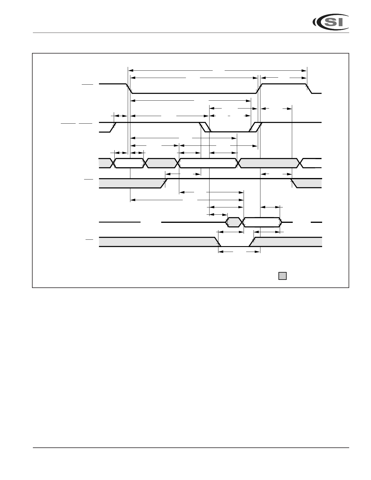
READ CYCLE
RAS
tCRP
UCAS-LCAS
tASR
ADDRESS
WE
I/O
OE
Row
tRAS
tRC
tRP
tRCD
tCSH
tRSH
tCAS tCLCH
tRRH
tRAD
tRAH
tASC
tAR
tRAL
Column
tRCS
tCAH
tRCH
Row
Open
tAA
tRAC
tCAC
tCLZ
tOE
tOFF(1)
Valid Data
Open
tOD
tOES
Note:
1. tOFF is referenced from rising edge of RAS or CAS, whichever occurs last.
Don’t Care
Integrated Circuit Solution Inc.
DR031-0A 10/17/2001
11
11 Page | ||
| Páginas | Total 19 Páginas | |
| PDF Descargar | [ Datasheet IC41C1665.PDF ] | |
Hoja de datos destacado
| Número de pieza | Descripción | Fabricantes |
| IC41C1665 | 64K x16 bit Dynamic RAM with Fast Page Mode | ICSI |
| Número de pieza | Descripción | Fabricantes |
| SLA6805M | High Voltage 3 phase Motor Driver IC. |
Sanken |
| SDC1742 | 12- and 14-Bit Hybrid Synchro / Resolver-to-Digital Converters. |
Analog Devices |
|
DataSheet.es es una pagina web que funciona como un repositorio de manuales o hoja de datos de muchos de los productos más populares, |
| DataSheet.es | 2020 | Privacy Policy | Contacto | Buscar |
