|
|
|
PDF ADS-930 Data sheet ( Hoja de datos )
| Número de pieza | ADS-930 | |
| Descripción | 16-Bit / 500kHz Sampling A/D Converters | |
| Fabricantes | Datel | |
| Logotipo | ||
Hay una vista previa y un enlace de descarga de ADS-930 (archivo pdf) en la parte inferior de esta página. Total 8 Páginas | ||
|
No Preview Available !
®®
INNOVATION and EXCELLENCE
ADS-930
16-Bit, 500kHz
Sampling A/D Converters
FEATURES
• 16-bit resolution
• 500kHz sampling rate
• Functionally complete
• Excellent dynamic performance
• 83dB SNR, –89dB THD
• No missing codes
• Small, 40-pin, TDIP package
• 3.5 Watts power dissipation
• On-board FIFO
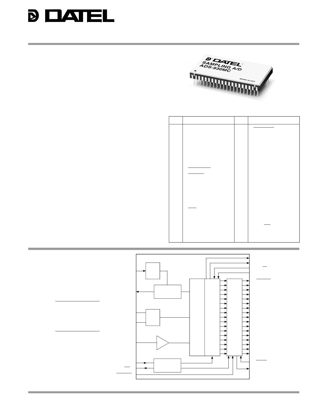
GENERAL DESCRIPTION
The low-cost ADS-930 is a high-performance, 16-bit, 500kHz
sampling A/D converter. This device accurately samples full-
scale input signals up to Nyquist frequencies with no missing
codes. The dynamic performance of the ADS-930 is optimized
to achieve a THD of –89dB and an SNR of 83dB.
Packaged in a small, 40-pin, ceramic TDIP, the functionally
complete ADS-930 contains a fast-settling sample-hold
amplifier, a subranging (three-pass) A/D converter, an internal
reference, an on-board FIFO, timing and control logic, three-
state outputs and error-correction circuitry. Digital inputs/
outputs are TTL.
Requiring ±15V and +5V supplies, the ADS-930 typically
dissipates 3.5 Watts. The unit is offered with a bipolar input
range of ±5V or a unipolar input range of 0 to –10V. Models
are available for use in either commercial (0 to +70°C) or
military (–55 to +125°C) operating temperature ranges.
Typical applications include radar, sonar, medical/graphic
imaging, and FFT spectrum analysis.
INPUT/OUTPUT CONNECTIONS
PIN FUNCTION
PIN FUNCTION
1 +10V REF. OUT
2 BIPOLAR
3 ANALOG INPUT
4 ANALOG GROUND
5 OFFSET ADJUST
6 GAIN ADJUST
7 +15V SUPPLY
8 COMP. BITS
9 ENABLE
10 FIFO READ
11 ANALOG GROUND
12 –15V SUPPLY
13 ANALOG GROUND
14 OVERFLOW
15 EOC
16 +5V SUPPLY
17 START CONVERT
18 DIGITAL GROUND
19 FSTAT1
20 FSTAT2
40 BIT 1 (MSB)
39 BIT 1 (MSB)
38 BIT 2
37 BIT 3
36 BIT 4
35 BIT 5
34 BIT 6
33 BIT 7
32 BIT 8
31 BIT 9
30 ANALOG GROUND
29 BIT 10
28 BIT 11
27 BIT 12
26 BIT 13
25 BIT 14
24 DIGITAL GROUND
23 FIFO/DIR
22 BIT 15
21 BIT 16 (LSB)
GAIN ADJUST 6
GAIN
ADJUST
CKT.
POWER AND GROUNDING
+5V SUPPLY
16
+15V SUPPLY
7
–15V SUPPLY
12
ANALOG GROUND 4, 11, 13, 30
DIGITAL GROUND
18, 24
+10V REF. OUT 1
OFFSET ADJUST 5
BIPOLAR 2
PRECISION
+10V REFERENCE
OFFSET
ADJUST
CKT.
ANALOG INPUT 3
S/H
START CONVERT 17
EOC 15
COMP. BITS 8
TIMING AND
CONTROL LOGIC
Figure 1. ADS-930 Functional Block Diagram
19 FSTAT1
20 FSTAT2
23 FIFO/DIR
10 FIFO READ
40 BIT 1 (MSB)
39 BIT 1 (MSB)
38 BIT 2
37 BIT 3
36 BIT 4
35 BIT 5
34 BIT 6
33 BIT 7
32 BIT 8
31 BIT 9
29 BIT 10
28 BIT 11
27 BIT 12
26 BIT 13
25 BIT 14
22 BIT 15
21 BIT 16 (LSB)
9 ENABLE
14 OVERFLOW
DATEL, Inc., 11 Cabot Boulevard, Mansfield, MA 02048 (U.S.A.) • Tel: (508)339-3000, (800)233-2765 Fax: (508)339-6356 • Email: [email protected]
1 page 
®®
ADS-930
CALIBRATION PROCEDURE
(Refer to Figure 2 and Tables 3a, and 3b)
Connect the converter per Table 2 for the appropriate input
voltage range. Any offset/gain calibration procedures should
not be implemented until the device is fully warmed up. To
avoid interaction, adjust offset before gain. The ranges of
adjustment for the circuits in Figure 2 are guaranteed to
compensate for the ADS-930's initial accuracy errors and may
not be able to compensate for additional system errors.
A/D converters are calibrated by positioning their digital
outputs exactly on the transition point between two adjacent
digital output codes. This is accomplished by connecting
LED's to the digital outputs and performing adjustments until
certain LED's "flicker" equally between on and off. Other
approaches employ digital comparators or microcontrollers to
detect when the outputs change from one code to the next.
For the ADS-930, offset adjusting is normally accomplished
when the analog input is 0 minus ½ LSB (–76µV). See Table
3b for the proper bipolar and unipolar output coding.
Gain adjusting is accomplished when the analog input is at
nominal full scale minus 1½ LSB's (–9.999771V for unipolar
and +4.999771V for bipolar).
Note: Connect pin 5 to ANALOG GROUND (pin 4) for
operation without zero/offset adjustment. Connect
pin 6 to pin 4 for operation without gain adjustment.
+5V
4.7µF
0.1µF
+15V
4.7µF
0.1µF
4.7µF
–15V
0.1µF
0.1µF
4.7µF
20kΩ
+15V
–15V
20kΩ
+15V
–15V
6
GAIN
ADJUST
16
+5V
DIGITAL
18, 24
DIGITAL
GROUND
5
OFFSET
ADJUST
7 +15V
4, 11 ANALOG
13, 30 GROUND
12 –15V
ADS-930
9 ENABLE
23 FIFO/DIR
19 FSTAT1
20 FSTAT2
2 BIPOLAR
1 +10V REF. OUT
ANALOG INPUT 3
FIFO READ 10
START CONVERT 17
COMP. BITS 8
15 EOC
14 OVERFLOW
40 BIT 1 (MSB)
39 BIT 1 (MSB)
38 BIT 2
37 BIT 3
36 BIT 4
35 BIT 5
34 BIT 6
33 BIT 7
32 BIT 8
31 BIT 9
29 BIT 10
28 BIT 11
27 BIT 12
26 BIT 13
25 BIT 14
22 BIT 15
21 BIT 16 (LSB)
+5V
Figure 2. Bipolar Connection Diagram
Zero/Offset Adjust Procedure
1. Apply a train of pulses to the START CONVERT input
(pin 17) so that the converter is continuously converting.
2. For unipolar or bipolar zero/offset adjust, apply –76.3µV to
the ANALOG INPUT (pin 3).
3. For a bipolar input - adjust the offset potentiometer until the
code flickers between 1000 0000 0000 0000 and 0111
1111 1111 1111 with pin 8 tied high (offset binary) or
between 0111 1111 1111 1111 and 1000 0000 0000 0000
with pin 8 tied low (complementary offset binary).
For a unipolar input - adjust the offset potentiometer until all
output bits are 0's and the LSB flickers between 0 and 1
with pin 8 tied high (straight binary) or until all output bits
are 1's and the LSB flickers between 0 and 1 with pin 8 tied
low (complementary binary).
4. Two's complement coding requires using BIT 1 (MSB) (pin
40). With pin 8 tied high, adjust the trimpot until the output
code flickers between all 0's and all 1's.
Table 2. Input Connections
INPUT RANGE
0 to –10V
±5V
INPUT PIN
Pin 3
Pin 3
TIE TOGETHER
Pins 2 and 4
Pins 1 and 2
Table 3a. Setting Output Coding Selection (Pin 8)
OUTPUT FORMAT
PIN 8 LOGIC LEVEL
Straight Binary
Complementary Binary
Complementary Offset Binary
Offset Binary
Complementary Two’s Complement
(Using MSB, pin 40)
Two’s Complement
(Using MSB, pin 40)
1
0
0
1
0
1
Table 3b. Output Coding
STRAIGHT BIN
COMP. BINARY
UNIPOLAR
SCALE
–FS +1 LSB
–FS +1 1/2 LSB
–7/8 FS
–3/4 FS
–1/2FS
–1/2FS –1/2LSB
–1/4FS
–1/8FS
–1 LSB
–1/2LSB
0
INPUT
RANGE
0 to –10V
–9.999847
–9.999771
–8.750000
–7.500000
–5.000000
–4.999924
–2.500000
–1.250000
–0.000153
–0.000076
0.000000
MSB
LSB
1111 1111 1111 1111
LSB "1" to "0"
1110 0000 0000 0000
1100 0000 0000 0000
1000 0000 0000 0000
0111 1111 1111 1111
0100 0000 0000 0000
0010 0000 0000 0000
0000 0000 0000 0001
LSB "0" to "1"
0000 0000 0000 0000
COMP. OFF. BIN.
OUTPUT CODING
MSB
LSB
0000 0000 0000 0000
LSB "0" to "1"
0001 1111 1111 1111
0011 1111 1111 1111
0111 1111 1111 1111
1000 0000 0000 0000
1011 1111 1111 1111
1101 1111 1111 1111
1111 1111 1111 1110
LSB "1" to "0"
1111 1111 1111 1111
OFFSET BINARY
MSB
LSB
0111 1111 1111 1111
LSB "1" to "0"
0110 0000 0000 0000
0100 0000 0000 0000
0000 0000 0000 0000
1111 1111 1111 1111
1100 0000 0000 0000
1010 0000 0000 0000
1000 0000 0000 0001
LSB "0" to "1"
1000 0000 0000 0000
COMP. TWO'S COMP.
MSB
LSB
1000 0000 0000 0000
LSB "0" to "1"
1001 1111 1111 1111
1011 1111 1111 1111
1111 1111 1111 1111
0000 0000 0000 0000
0011 1111 1111 1111
0101 1111 1111 1111
0111 1111 1111 1110
LSB "1" to "0"
01111111 1111 1111
TWO'S COMP.
INPUT
RANGE
±5V
+4.999847
+4.999771
+3.750000
+2.500000
0.000000
–0.000076
–2.500000
–3.750000
–4.999847
–4.999924
–5.000000
BIPOLAR
SCALE
+FS –1 LSB
+FS –1 1/2 LSB
+3/4 FS
+1/2 FS
0
–1/2 LSB
–1/2 FS
–3/4 FS
–FS +1 LSB
–FS + 1/2 LSB
–FS
5
5 Page | ||
| Páginas | Total 8 Páginas | |
| PDF Descargar | [ Datasheet ADS-930.PDF ] | |
Hoja de datos destacado
| Número de pieza | Descripción | Fabricantes |
| ADS-930 | 16-Bit / 500kHz Sampling A/D Converters | Datel |
| ADS-931 | A/D Converters | Datel |
| ADS-932 | A/D Converters | Datel |
| ADS-933 | 16-Bit / 3MHz Sampling A/D Converters | Datel |
| Número de pieza | Descripción | Fabricantes |
| SLA6805M | High Voltage 3 phase Motor Driver IC. |
Sanken |
| SDC1742 | 12- and 14-Bit Hybrid Synchro / Resolver-to-Digital Converters. |
Analog Devices |
|
DataSheet.es es una pagina web que funciona como un repositorio de manuales o hoja de datos de muchos de los productos más populares, |
| DataSheet.es | 2020 | Privacy Policy | Contacto | Buscar |