|
|
|
PDF L64733C Data sheet ( Hoja de datos )
| Número de pieza | L64733C | |
| Descripción | (L64734) Tuner and Satellite Receiver Chipset | |
| Fabricantes | LSI Logic | |
| Logotipo | ||
Hay una vista previa y un enlace de descarga de L64733C (archivo pdf) en la parte inferior de esta página. Total 52 Páginas | ||
|
No Preview Available !
L64733C/L64734 Tuner and
Satellite Receiver Chipset
Datasheet
®
The L64733C/734 chipset is designed for satellite broadcast digital TV. It
is compliant with the European digital video broadcast (DVB-S) standard,
as well as the technical specifications for DSS systems. The
L64733C/734 chipset forms a complete “L-band-to-bits” system.
A typical application of the L64733C/734 chipset is satellite digital TV
reception in accordance with the ETS 300 421 standard. Figure 1 shows
the L64733C/734 chipset satellite receiver implemented in a typical
satellite receiver set-top decoder.
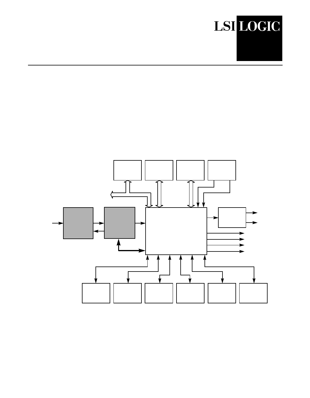
Figure 1 Set-Top Box Block Diagram
FLASH
SDRAM-B SDRAM-A
27 MHz
VCXO
Expansion
Bus
Satellite
RF Signal
L64733C
Tuner
L64734
Demodulator
Serial Bus
SC2000
Single-Chip
Source Decoder
OP
AMPs
Analog
Audio
Analog CVBS
Analog Y/C
Analog RGB
Digital Video
IEEE
1284
Smart
Cards
RS232-C
Interface
CODEC
I/R
Rx & Tx
GPIO
Pins
The L64733C Tuner IC directly down-converts the satellite signal from
L-band to baseband; it includes an on-chip synthesizer. Using frequency
information programmed into its configuration registers, the L64734
Satellite Receiver generates control signals for the L64733C synthesizer.
The L64734 also controls the programming of the low-pass filters on the
February 2001
Copyright © 2000, 2001 by LSI Logic Corporation. All rights reserved.
1
1 page 
has 3-state operation (see the “Synthesizer Control Interface” section on
page 20).
The VCO requires an external resonant tank circuit, which includes
varactor diodes to vary the frequency of oscillation.
The VCO signal is fed to the Prescaler block before being passed
deferentially through the PSOUTp and PSOUTn pins to the L64734. The
L64734 MODp and MODn differential signals control the divider ratio for
the Prescaler block. The L64734 dynamically changes the divide ratio to
ensure that the tuning step size is not affected by the divider. The
L64734 contains programmable counters to further divide the signal
frequency before it is fed back to the L64733C through the PLLINp and
PLLINn pins. The crystal reference oscillator frequency is divided by
eight and fed to the phase detector. The phase detector generates a
current signal proportional to the difference in phase between PLLINp,
PLLINn, and the divided crystal frequency. A charge pump circuit
generates current that controls pins CP and FB, and an external
transistor to buffer the L64733C against the tuning voltage (28 V). The
current is passed through a discrete loop filter and is converted to a
tuning voltage that drives the external varactor diodes for the VCO tank
circuit. A frequency controlled loop is formed. Changing the frequency
divider ratios in the L64734 registers varies the VCO frequency. See
Figure 7, on page 23, for more details regarding the external circuitry for
the VCO, crystal oscillator, charge pump, tank circuitry, and
frequency-controlled loop.
The chipset provides maximum integration and flexibility for system
designers at a minimum cost. The number of external components
required to build a system is minimal because the synthesizer, variable
rate filters, and clock and carrier loops are integrated into the two
devices.
L64733C/L64734 Tuner and Satellite Receiver Chipset
5
5 Page 
QOUTp, QOUTn
Q Channel Baseband Data
Output
The QOUT differential signals form the quadrature-phase
data provided to the L64734.
Prescaler Signals
The following signals are the prescaler outputs from the L64733C to the
L64734.
PSOUTp, PSOUTn
Prescaler
Output
When the LOBUF signal is LOW, the PSOUT differential
signals are the L64733C prescaler outputs.
When LOBUF is HIGH, the Local Oscillator (LO) buffer
(50 Ω) feeds the PSOUT differential signals.
The programmable counters on the L64734 are clocked
on the rising edge of the PSOUT signal.
Control Signals
The following signals, some of which are generated by the L64734 IC,
control the mode of operation of the L64733C IC.
AGC1
Automatic Gain Control 1
Input
The AGC1 signal is a high-impedance input from the
L64734 that controls RF AGC circuitry. The AGC1 voltage
has a range of 0.5 V to 4.8 V.
AGC2
Automatic Gain Control 2
Input
The AGC2 signal is a high-impedance input from the
L64734 that controls RF AGC circuitry.
CPG[2:1]
Charge Pump Gain
The CPG[2:1] signals set the charge pump gain
according to the table below.
Input
CPG1
0
0
1
1
CPG2
0
1
0
1
Charge Pump Current (typ), mA
FB HIGH
FB LOW
0.1 −0.1
0.3 −0.3
0.6 −0.6
1.8 −1.8
L64733C/L64734 Tuner and Satellite Receiver Chipset
11
11 Page | ||
| Páginas | Total 52 Páginas | |
| PDF Descargar | [ Datasheet L64733C.PDF ] | |
Hoja de datos destacado
| Número de pieza | Descripción | Fabricantes |
| L64733C | (L64734) Tuner and Satellite Receiver Chipset | LSI Logic |
| Número de pieza | Descripción | Fabricantes |
| SLA6805M | High Voltage 3 phase Motor Driver IC. |
Sanken |
| SDC1742 | 12- and 14-Bit Hybrid Synchro / Resolver-to-Digital Converters. |
Analog Devices |
|
DataSheet.es es una pagina web que funciona como un repositorio de manuales o hoja de datos de muchos de los productos más populares, |
| DataSheet.es | 2020 | Privacy Policy | Contacto | Buscar |