|
|
|
PDF CH7012A Data sheet ( Hoja de datos )
| Número de pieza | CH7012A | |
| Descripción | Chrontel CH7012 TV Output Device | |
| Fabricantes | ETC | |
| Logotipo | ||
Hay una vista previa y un enlace de descarga de CH7012A (archivo pdf) en la parte inferior de esta página. Total 42 Páginas | ||
|
No Preview Available !
CHRONTEL
CH7012A
Chrontel CH7012 TV Output Device
Features
• TV output supporting up to 1024x768 graphics
resolutions
• Programmable digital interface supports RGB and
YCrCb
• TrueScaleTM rendering engine supports underscan in
all TV output resolutions
• Enhanced text sharpness and adaptive flicker
removal with up to 7 lines of filtering
• Support for all NTSC and PAL formats
• Provides CVBS, S-Video and SCART (RGB) outputs
• TV connection detect
• Programmable power management
• 10-bit video DAC outputs
• Fully programmable through serial port
• Complete Windows and DOS driver support
• Low voltage interface support to graphics device
• Offered in a 64-pin LQFP package
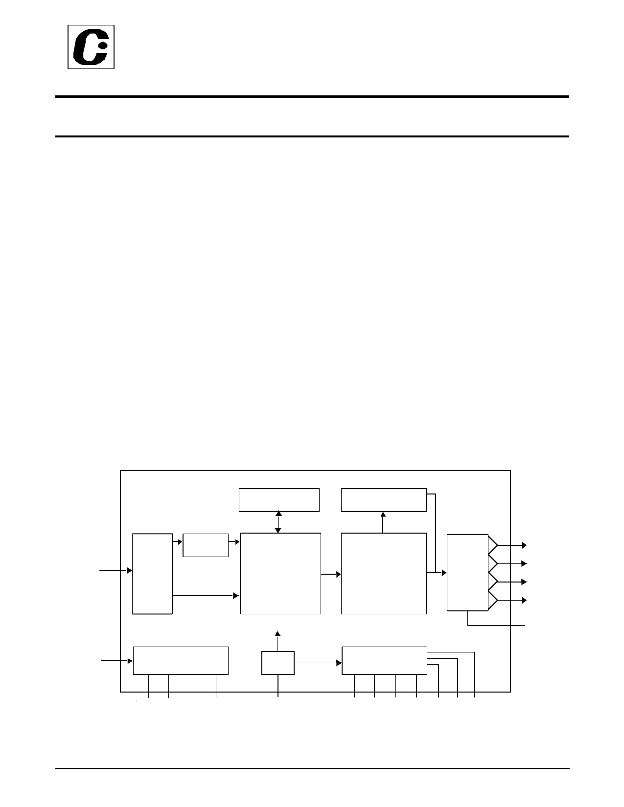
General Description
The CH7012 is a display controller device which
accepts a digital graphics input signal, and encodes and
transmits data to a TV output (analog composite, s-
video or RGB). The device accepts data over one 12-bit
wide variable voltage data port which supports five
different data formats including RGB and YCrCb.
The TV-Out processor will perform non-interlace to
interlace conversion with scaling and flicker filters, and
encode the data into any of the NTSC or PAL video
standards. The scaling and flicker filter is adaptive and
programmable to enable superior text display. Eight
graphics resolutions are supported up to 1024 by 768
with full vertical and horizontal underscan capability in
all modes. A high accuracy low jitter phase locked loop
is integrated to create outstanding video quality.
Support is provided for RGB bypass mode which
enables driving a VGA CRT with the input data.
LINE
MEMORY
D [11:0]
PIXEL DATA
DIGITAL
INPUT
INTERFACE
RGB-YUV
CONVERTER
TRUE SCALE
SCALING &
DEFLICKERING
ENGINE
YUV-RGB CONVERTER
NTSC/PAL
ENCODER
& FILTERS
Four
10-bit
DAC’s
GPIO[1:0]
SERIAL PORT REGISTER &
CONTROL BLOCK
SYSTEM CLOCK
PLL
TIMING & SYNC
GENERATOR
SC SD
RESET*
XCLK/XCLK*
H V XI/FIN XO CSYNC P-OUT BCO
Figure 1: Functional Block Diagram
201-0000-042 Rev. 1.1, 9/29/2000
CVBS
Y/R
C/G
CVBS/B
ISET
1
1 page 
CHRONTEL
Table 1: Pin Description
64-Pin
LQFP
57, 56
# Pins Type
2 In
2, 9, 19, 21, 11
23, 24, 25,
27, 28, 30,
31
1, 12, 49
3
6, 11, 64 3
45
23, 29
20, 26, 32
18, 44
1
2
3
2
16, 17, 41 3
33 1
34, 40
2
Power
Power
Power
Power
Power
Power
Power
Power
Power
CH7012A
Symbol Description
XCLK,
XCLK*
NC
External Clock Inputs
These inputs form a differential clock signal input to the
CH7012 for use with the H, V, DE and D[11:0] data. If
differential clocks are not available, the XCLK* input
should be connected to VREF.
The output clocks from this pad cell are able to have their
polarities reversed under the control of the MCP bit.
No Connect
DVDD
DGND
DVDDV
NC
NC
AVDD
AGND
VDD
GND
Digital Supply Voltage (3.3V)
Digital Ground
I/O Supply Voltage (3.3V to 1.1V)
No Connect
No Connect
PLL Supply Voltage (3.3V)
PLL Ground
DAC Supply Voltage (3.3V)
DAC Ground
201-0000-042 Rev. 1.1, 9/29/2000
5
5 Page 
CHRONTEL
CH7012A
HS
XCLK
(2X)
XCLK
(1X)
D[11:0]
SAV
P0a P0b P1a P1b P2a P2b
P[23:19]
(Red Data)
P[15:10]
(Green Data)
P[7:3]
(Blue Data)
The following data is latched for IDF = 2
P0b[11:7]
P0b[6:4], P0a[11:9]
P0a[8:4]
P1b[11:7]
P1b[6:4], P1a[11:9]
P1a[8:4]
P2b[11:7]
P2b[6:4],
P2a[11:9]
P2a[8:4]
P[23:19]
(Red Data)
P[15:11]
(Green Data)
P[7:3]
(Blue Data)
The following data is latched for IDF = 3
CRA
(internal signal)
P[23:16]
(Y Data)
P[15:8]
(CrCb Data)
P[7:0]
(ignored)
The following data is latched for IDF = 4
P0b[10:6]
P0b[5:4], P0a[11:9]
P0a[8:4]
P1b[10:6]
P1b[5:4], P1a[11:9]
P1a[8:4]
P2b[10:6]
P2b[5:4],
P2a[11:9]
P2a[8:4]
P0b[7:0]
P0a[7:0]
GND
P1b[7:0]
P1a[7:0]
GND
P2b[7:0]
P2a[7:0]
GND
Figure 6: Multiplexed Input Data Formats (IDF = 2, 3, 4)
201-0000-042 Rev. 1.1, 9/29/2000
11
11 Page | ||
| Páginas | Total 42 Páginas | |
| PDF Descargar | [ Datasheet CH7012A.PDF ] | |
Hoja de datos destacado
| Número de pieza | Descripción | Fabricantes |
| CH7012A | Chrontel CH7012 TV Output Device | ETC |
| Número de pieza | Descripción | Fabricantes |
| SLA6805M | High Voltage 3 phase Motor Driver IC. |
Sanken |
| SDC1742 | 12- and 14-Bit Hybrid Synchro / Resolver-to-Digital Converters. |
Analog Devices |
|
DataSheet.es es una pagina web que funciona como un repositorio de manuales o hoja de datos de muchos de los productos más populares, |
| DataSheet.es | 2020 | Privacy Policy | Contacto | Buscar |