|
|
|
PDF TC7135 Data sheet ( Hoja de datos )
| Número de pieza | TC7135 | |
| Descripción | 4-1/2 Digit A/D Converter | |
| Fabricantes | Microchip | |
| Logotipo | ||
Hay una vista previa y un enlace de descarga de TC7135 (archivo pdf) en la parte inferior de esta página. Total 22 Páginas | ||
|
No Preview Available !
TC7135
4-1/2 Digit A/D Converter
Features
• Low Rollover Error: ±1 Count Max
• Nonlinearity Error: ±1 Count Max
• Reading for 0V Input
• True Polarity Indication at Zero for Null Detection
• Multiplexed BCD Data Output
• TTL-Compatible Outputs
• Differential Input
• Control Signals Permit Interface to UARTs and
Microprocessors
• Blinking Display Visually Indicates Overrange
Condition
• Low Input Current: 1pA
• Low Zero Reading Drift: 2µV/°C
• Auto-Ranging Supported with Overrange and
Underrange Signals
• Available in PDIP and Surface-Mount Packages
Applications
• Precision Analog Signal Processor
• Precision Sensor Interface
• High Accuracy DC Measurements
Device Selection Table
Part Number
TC7135CLI
TC7135CPI
TC7135CBU
Package
28-Pin PLCC
28-Pin PDIP
64-Pin PQFP
Temperature Range
0°C to +70°C
0°C to +70°C
0°C to +70°C
General Description
The TC7135 4-1/2 digit A/D converter (ADC) offers
50ppm (1 part in 20,000) resolution with a maximum
nonlinearity error of 1 count. An auto zero cycle
reduces zero error to below 10µV and zero drift to
0.5µV/°C. Source impedance errors are minimized by
a 10pA maximum input current. Rollover error is limited
to ±1 count.
Microprocessor based measurement systems are sup-
ported by BUSY, STROBE and RUN/HOLD control sig-
nals. Remote data acquisition systems with data
transfer via UARTs are also possible. The additional
control pins and multiplexed BCD outputs make the
TC7135 the ideal converter for display or
microprocessor based measurement systems.
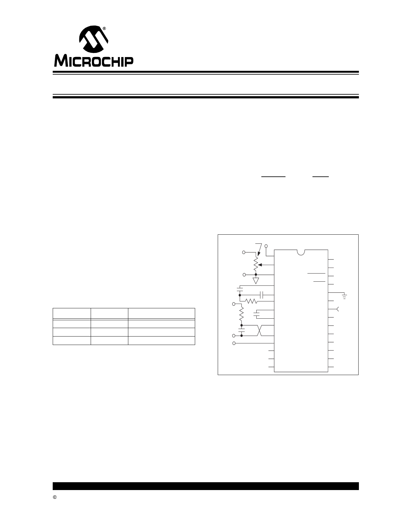
Functional Block Diagram
SET VREF = 1V –5V
TC7135
VREF IN
100kΩ
Analog GND
0.47µF
1
2
V-
REF IN
UNDERRANGE
OVERRANGE
28
27
3 ANALOG
26
COMMON STROBE
1µF
4
5
6
INT OUT RUN/HOLD
AZ IN DIGTAL GND
BUFF OUT POLARITY
25
24
23
Signal
Input
100kΩ
100
kΩ
7
1µF 8
9
CREF-
CREF+
-INPUT
22
CLOCK IN
21
BUSY
(LSD) D1 20
0.1µF 10 +INPUT
+5V 11 V+
19
D2
D3 18
12 D5 (MSD)
D4 17
13 B1 (LSB) (MSB) B8 16
14 B2
B4 15
Clock
Input
120kHz
© 2002 Microchip Technology Inc.
DS21460B-page 1
1 page 
TC7135
2.0 PIN DESCRIPTIONS
The description of the pins are listed in Table 2-1.
TABLE 2-1: PIN FUNCTION TABLE
Pin Number
28-Pin PDIP
1
2
3
4
5
6
7
8
9
10
11
12
13
14
15
16
17
18
19
20
21
22
23
24
25
26
27
28
Symbol
Description
V-
REF IN
ANALOG COMMON
INT OUT
AZ IN
BUFF OUT
CREF-
CREF+
-INPUT
+INPUT
V+
D5
B1
B2
B4
B8
D4
D3
D2
D1
BUSY
CLOCK IN
POLARITY
DGND
RUN/HOLD
STROBE
OVERRANGE
UNDERRANGE
Negative power supply input.
External reference input.
Reference point for REF IN.
Integrator output. Integrator capacitor connection.
Auto zero inpt. Auto-zero capacitor connection.
Analog input buffer output. Integrator resistor connection.
Reference capacitor input. Reference capacitor negative connection.
Reference capacitor input. Reference capacitor positive connection.
Analog input. Analog input negative connection.
Analog input. Analog input positive connection.
Positive power supply input.
Digit drive output. Most Significant Digit (MSD)
Binary Coded Decimal (BCD) output. Least Significant Bit (LSB)
BCD output.
BCD output.
BCD output. Most Significant Bit (MSB)
Digit drive output.
Digit drive output.
Digit drive output.
Digit drive output. Least Significant Digit (LSD)
Busy output. At the beginning of the signal-integration phase, BUSY goes High and
remains High until the first clock pulse after the integrator zero crossing.
Clock input. Conversion clock connection.
Polarity output. A positive input is indicated by a logic High output. The polarity output is
valid at the beginning of the reference integrate phase and remains valid until determined
during the next conversion.
Digital logic reference input.
Run / Hold input. When at a logic High, conversions are performed continuously. A logic
Low holds the current data as long as the Low condition exists.
Strobe output. The STROBE output pulses low in the center of the digit drive outputs.
Over range output. A logic High indicates that the analog input exceeds the full scale input
range.
Under range output. A logic High indicates that the analog input is less than 9% of the full
scale input range.
© 2002 Microchip Technology Inc.
DS21460B-page 5
5 Page 
5.3 BUSY Output
At the beginning of the signal integration phase, BUSY
goes high and remains high until the first clock pulse
after the integrator zero crossing. BUSY returns to the
logic "0" state after the measurement cycle ends in an
overrange condition. The internal display latches are
loaded during the first clock pulse after BUSY and are
latched at the clock pulse end. The BUSY signal does
not go high at the beginning of the measurement cycle,
which starts with the auto zero cycle.
5.4 OVERRANGE Output
If the input signal causes the reference voltage integra-
tion time to exceed 20,000 clock pulses, the OVER-
RANGE output is set to a logic "1." The overrange
output register is set when BUSY goes low and is reset
at the beginning of the next reference integration
phase.
5.5 UNDERRANGE Output
If the output count is 9% of full scale or less (-1800
counts), the underrange register bit is set at the end of
BUSY. The bit is set low at the next signal integration
phase.
5.6 POLARITY Output
A positive input is registered by a logic "1" polarity sig-
nal. The polarity bit is valid at the beginning of refer-
ence integrate and remains valid until determined
during the next conversion.
The polarity bit is valid even for a zero reading. Signals
less than the converter's LSB will have the signal polar-
ity determined correctly. This is useful in null
applications.
5.7 Digit Drive Outputs
Digit drive signals are positive-going signals. The scan
sequence is D5 to D1. All positive pulses are 200 clock
pulses wide, with the exception D5, which is 201 clock
pulses wide.
All five digits are scanned continuously, unless an
overrange condition occurs. In an overrange condition,
all digit drives are held low from the final STROBE
pulse until the beginning of the next reference integrate
phase. The scanning sequence is then repeated. This
provides a blinking visual display indication.
5.8 BCD Data Outputs
The binary coded decimal (BCD) bits B8, B4, B2, and B1
are positive-true logic signals. The data bits become
active at the same time as the digit drive signals. In an
overrange condition, all data bits are at a logic "0" state.
© 2002 Microchip Technology Inc.
TC7135
DS21460B-page 11
11 Page | ||
| Páginas | Total 22 Páginas | |
| PDF Descargar | [ Datasheet TC7135.PDF ] | |
Hoja de datos destacado
| Número de pieza | Descripción | Fabricantes |
| TC7135 | 4-1/2 Digit A/D Converter | Microchip |
| TC7135 | 4-1/2 DIGIT ANALOG-TO-DIGITAL CONVERTER | TelCom |
| TC7136 | Low Power 3-1/2 Digit Analog-to-Digital Converter | Microchip |
| TC7136 | LOW POWER 3-1/2 DIGIT ANALOG-TO-DIGITAL CONVERTERS | TelCom |
| Número de pieza | Descripción | Fabricantes |
| SLA6805M | High Voltage 3 phase Motor Driver IC. |
Sanken |
| SDC1742 | 12- and 14-Bit Hybrid Synchro / Resolver-to-Digital Converters. |
Analog Devices |
|
DataSheet.es es una pagina web que funciona como un repositorio de manuales o hoja de datos de muchos de los productos más populares, |
| DataSheet.es | 2020 | Privacy Policy | Contacto | Buscar |