|
|
|
PDF IRFSL3307 Data sheet ( Hoja de datos )
| Número de pieza | IRFSL3307 | |
| Descripción | HEXFET Power MOSFET | |
| Fabricantes | IRF | |
| Logotipo | ||
Hay una vista previa y un enlace de descarga de IRFSL3307 (archivo pdf) en la parte inferior de esta página. Total 11 Páginas | ||
|
No Preview Available !
Applications
l High Efficiency Synchronous Rectification in SMPS
l Uninterruptible Power Supply
l High Speed Power Switching
l Hard Switched and High Frequency Circuits
Benefits
l Improved Gate, Avalanche and Dynamic dV/dt
Ruggedness
l Fully Characterized Capacitance and Avalanche
SOA
l Enhanced body diode dV/dt and dI/dt Capability
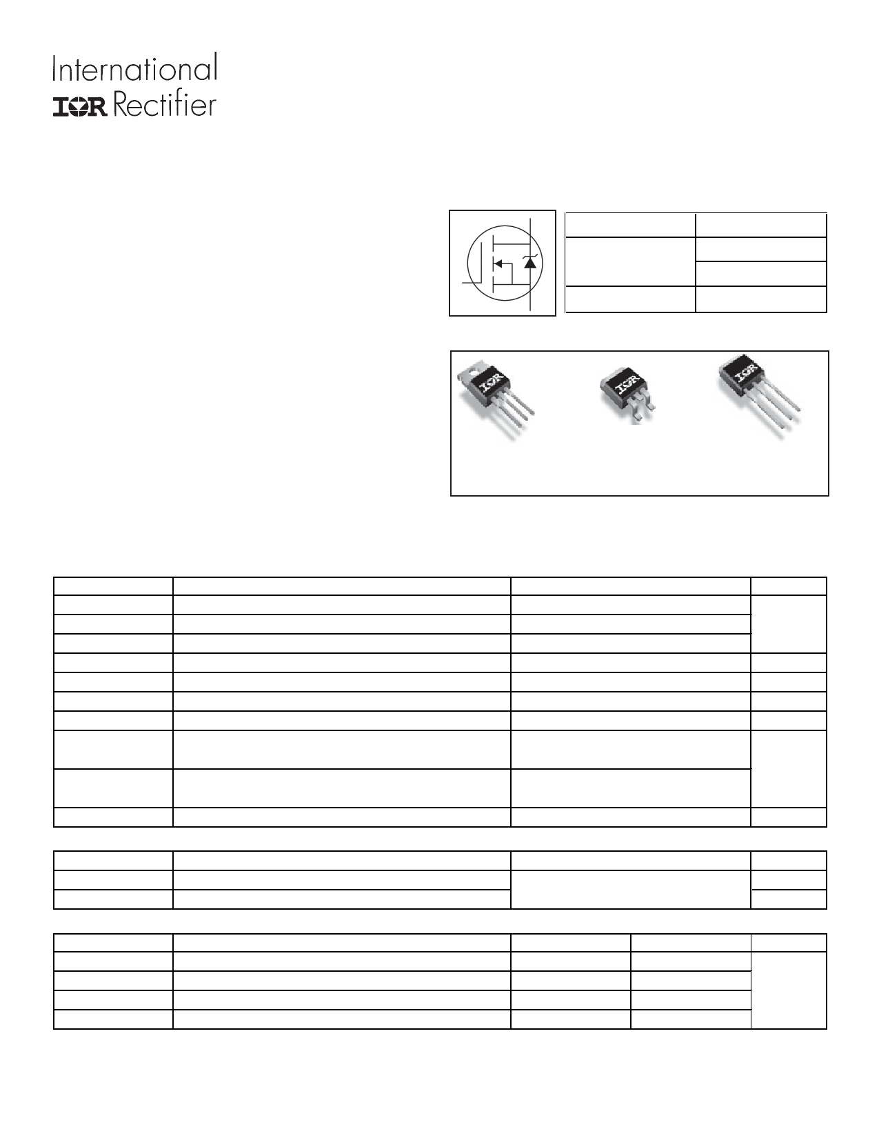
G
PD - 96901A
IRFB3307
IRFS3307
IRFSL3307
HEXFET® Power MOSFET
D VDSS
RDS(on) typ.
max.
S ID
75V
5.0m:
6.3m:
130A
G DS
TO-220AB
IRFB3307
G DS
D2Pak
IRFS3307
G DS
TO-262
IRFSL3307
Absolute Maximum Ratings
Symbol
Parameter
ID @ TC = 25°C
ID @ TC = 100°C
IDM
PD @TC = 25°C
Continuous Drain Current, VGS @ 10V
Continuous Drain Current, VGS @ 10V
Pulsed Drain Current d
Maximum Power Dissipation
Linear Derating Factor
VGS Gate-to-Source Voltage
dv/dt
Peak Diode Recovery f
TJ
TSTG
Operating Junction and
Storage Temperature Range
Soldering Temperature, for 10 seconds
(1.6mm from case)
Mounting torque, 6-32 or M3 screw
Avalanche Characteristics
EAS (Thermally limited)
Single Pulse Avalanche Energy e
IAR Avalanche Current c
EAR Repetitive Avalanche Energy g
Thermal Resistance
Symbol
Parameter
RθJC
Junction-to-Case k
RθCS
RθJA
RθJA
Case-to-Sink, Flat Greased Surface , TO-220
Junction-to-Ambient, TO-220 k
Junction-to-Ambient (PCB Mount) , D2Pak jk
www.irf.com
Max.
130c
91c
510
250
1.6
± 20
11
-55 to + 175
300
10lbxin (1.1Nxm)
270
See Fig. 14, 15, 16a, 16b
Typ.
–––
0.50
–––
–––
Max.
0.61
–––
62
40
Units
A
W
W/°C
V
V/ns
°C
mJ
A
mJ
Units
°C/W
1
11/04/04
1 page 
IRFB3307/IRFS3307/IRFSL3307
1
D = 0.50
0.1 0.20
0.10
0.05
0.01
0.001
0.02
0.01
SINGLE PULSE
( THERMAL RESPONSE )
0.0001
1E-006
1E-005
0.0001
τJ τJ
τ1 τ1
R1R1
CiC= iτi/Ri/iRi
R2R2
τ2 τ2
τCτ
Ri (°C/W) τi (sec)
0.2911 0.000484
0.3196 0.005529
Notes:
1. Duty Factor D = t1/t2
2. Peak Tj = P dm x Zthjc + Tc
0.001
0.01
0.1
1
t1 , Rectangular Pulse Duration (sec)
Fig 13. Maximum Effective Transient Thermal Impedance, Junction-to-Case
1000
Duty Cycle = Single Pulse
100 0.01
0.05
10 0.10
Allowed avalanche Current vs
avalanche pulsewidth, tav
assuming ∆ Tj = 25°C due to
avalanche losses
1
0.1
1.0E-06
1.0E-05
1.0E-04
1.0E-03
tav (sec)
Fig 14. Typical Avalanche Current vs.Pulsewidth
1.0E-02
1.0E-01
300
TOP
Single Pulse
Notes on Repetitive Avalanche Curves , Figures 14, 15:
(For further info, see AN-1005 at www.irf.com)
BOTTOM 1% Duty Cycle
1. Avalanche failures assumption:
250 ID = 75A
Purely a thermal phenomenon and failure occurs at a temperature far in
excess of Tjmax. This is validated for every part type.
200
2. Safe operation in Avalanche is allowed as long asTjmax is not exceeded.
3. Equation below based on circuit and waveforms shown in Figures 16a, 16b.
4. PD (ave) = Average power dissipation per single avalanche pulse.
150 5. BV = Rated breakdown voltage (1.3 factor accounts for voltage increase
during avalanche).
6. Iav = Allowable avalanche current.
100 7. ∆T = Allowable rise in junction temperature, not to exceed Tjmax (assumed as
25°C in Figure 14, 15).
tav = Average time in avalanche.
50 D = Duty cycle in avalanche = tav ·f
ZthJC(D, tav) = Transient thermal resistance, see Figures 13)
0
25 50 75 100 125 150 175
Starting TJ , Junction Temperature (°C)
PD (ave) = 1/2 ( 1.3·BV·Iav) = DT/ ZthJC
Iav = 2DT/ [1.3·BV·Zth]
EAS (AR) = PD (ave)·tav
Fig 15. Maximum Avalanche Energy vs. Temperature
www.irf.com
5
5 Page 
IRFB3307/IRFS3307/IRFSL3307
D2Pak Tape & Reel Information
TRR
1.60 (.063)
1.50 (.059)
4.10 (.161)
3.90 (.153)
FEED DIRECTION 1.85 (.073)
1.65 (.065)
TRL
10.90 (.429)
10.70 (.421)
1.60 (.063)
1.50 (.059)
11.60 (.457)
11.40 (.449)
15.42 (.609)
15.22 (.601)
1.75 (.069)
1.25 (.049)
16.10 (.634)
15.90 (.626)
0.368 (.0145)
0.342 (.0135)
24.30 (.957)
23.90 (.941)
4.72 (.136)
4.52 (.178)
FEED DIRECTION
13.50 (.532)
12.80 (.504)
27.40 (1.079)
23.90 (.941)
4
330.00
(14.173)
MAX.
60.00 (2.362)
MIN.
NOTES :
1. COMFORMS TO EIA-418.
2. CONTROLLING DIMENSION: MILLIMETER.
3. DIMENSION MEASURED @ HUB.
4. INCLUDES FLANGE DISTORTION @ OUTER EDGE.
26.40 (1.039)
24.40 (.961)
3
30.40 (1.197)
MAX.
4
Data and specifications subject to change without notice.
This product has been designed and qualified for the Automotive [Q101] market.
Qualification Standards can be found on IR’s Web site.
www.irf.com
IR WORLD HEADQUARTERS: 233 Kansas St., El Segundo, California 90245, USA Tel: (310) 252-7105
TAC Fax: (310) 252-7903
Visit us at www.irf.com for sales contact information. 11/04
11
11 Page | ||
| Páginas | Total 11 Páginas | |
| PDF Descargar | [ Datasheet IRFSL3307.PDF ] | |
Hoja de datos destacado
| Número de pieza | Descripción | Fabricantes |
| IRFSL3306PBF | Power MOSFET ( Transistor ) | International Rectifier |
| IRFSL3307 | HEXFET Power MOSFET | IRF |
| IRFSL3307 | HEXFET Power MOSFET | International Rectifier |
| IRFSL3307PbF | HEXFET Power MOSFET | International Rectifier |
| Número de pieza | Descripción | Fabricantes |
| SLA6805M | High Voltage 3 phase Motor Driver IC. |
Sanken |
| SDC1742 | 12- and 14-Bit Hybrid Synchro / Resolver-to-Digital Converters. |
Analog Devices |
|
DataSheet.es es una pagina web que funciona como un repositorio de manuales o hoja de datos de muchos de los productos más populares, |
| DataSheet.es | 2020 | Privacy Policy | Contacto | Buscar |