|
|
|
PDF HI3-5043-5 Data sheet ( Hoja de datos )
| Número de pieza | HI3-5043-5 | |
| Descripción | CMOS Analog Switches | |
| Fabricantes | Intersil | |
| Logotipo | ||
Hay una vista previa y un enlace de descarga de HI3-5043-5 (archivo pdf) en la parte inferior de esta página. Total 11 Páginas | ||
|
No Preview Available !
TM
Data Sheet
HI-5042 thru HI-5051
April 2000 File Number 3127.4
CMOS Analog Switches
This family of CMOS analog switches offers low resistance
switching performance for analog voltages up to the supply
rails and for signal currents up to 80mA. “ON” resistance is
low and stays reasonably constant over the full range of
operating signal voltage and current. rON remains
exceptionally constant for input voltages between +5V and
-5V and currents up to 50mA. Switch impedance also
changes very little over temperature, particularly between
0oC and 75oC. rON is nominally 25Ω for HI-5049 and
HI-5051 and 50Ω for HI-5042 through HI-5047.
All devices provide break-before-make switching and are
TTL and CMOS compatible for maximum application
versatility. Performance is further enhanced by Dielectric
Isolation processing which insures latch-free operation with
very low input and output leakage currents (0.8nA at 25oC).
This family of switches also features very low power
operation (1.5mW at 25oC).
There are 7 devices in this switch series which are
differentiated by type of switch action and value of rON (see
Functional Description Table). The HI-504X and HI-505X
series switches can directly replace IH-5040 series devices,
and are functionally compatible with the DG180 and DG190
family.
Ordering Information
PART
NUMBER
TEMP. RANGE
(oC)
PACKAGE
HI1-5042-2
HI1-5043-2
HI1-5043-5
HI3-5043-5
HI9P5043-5
HI1-5047-5
HI1-5049-5
HI1-5051-2
HI1-5051-5
-55 to 125
-55 to 125
0 to 75
0 to 75
0 to 75
0 to 75
0 to 75
-55 to 125
0 to 75
16 Ld CERDIP
16 Ld CERDIP
16 Ld CERDIP
16 Ld PDIP
16 Ld SOIC
16 Ld CERDIP
16 Ld CERDIP
16 Ld CERDIP
16 Ld CERDIP
HI3-5051-5
HI9P5051-9
0 to 75
-40 to 85
16 Ld PDIP
16 Ld SOIC
PKG. NO.
F16.3
F16.3
F16.3
E16.3
M16.15
F16.3
F16.3
F16.3
F16.3
E16.3
M16.15
Features
• Wide Analog Signal Range . . . . . . . . . . . . . . . . . . . ±15V
• Low “ON” Resistance . . . . . . . . . . . . . . . . . . . . . . . . . 25Ω
• High Current Capability . . . . . . . . . . . . . . . . . . . . . . 80mA
• Break-Before-Make Switching
- Turn-On Time . . . . . . . . . . . . . . . . . . . . . . . . . . . . 370ns
- Turn-Off Time . . . . . . . . . . . . . . . . . . . . . . . . . . . 280ns
• No Latch-Up
• Input MOS Gates are Protected from Electrostatic
Discharge
• DTL, TTL, CMOS, PMOS Compatible
Applications
• High Frequency Switching
• Sample and Hold
• Digital Filters
• Operational Amplifier Gain Switching
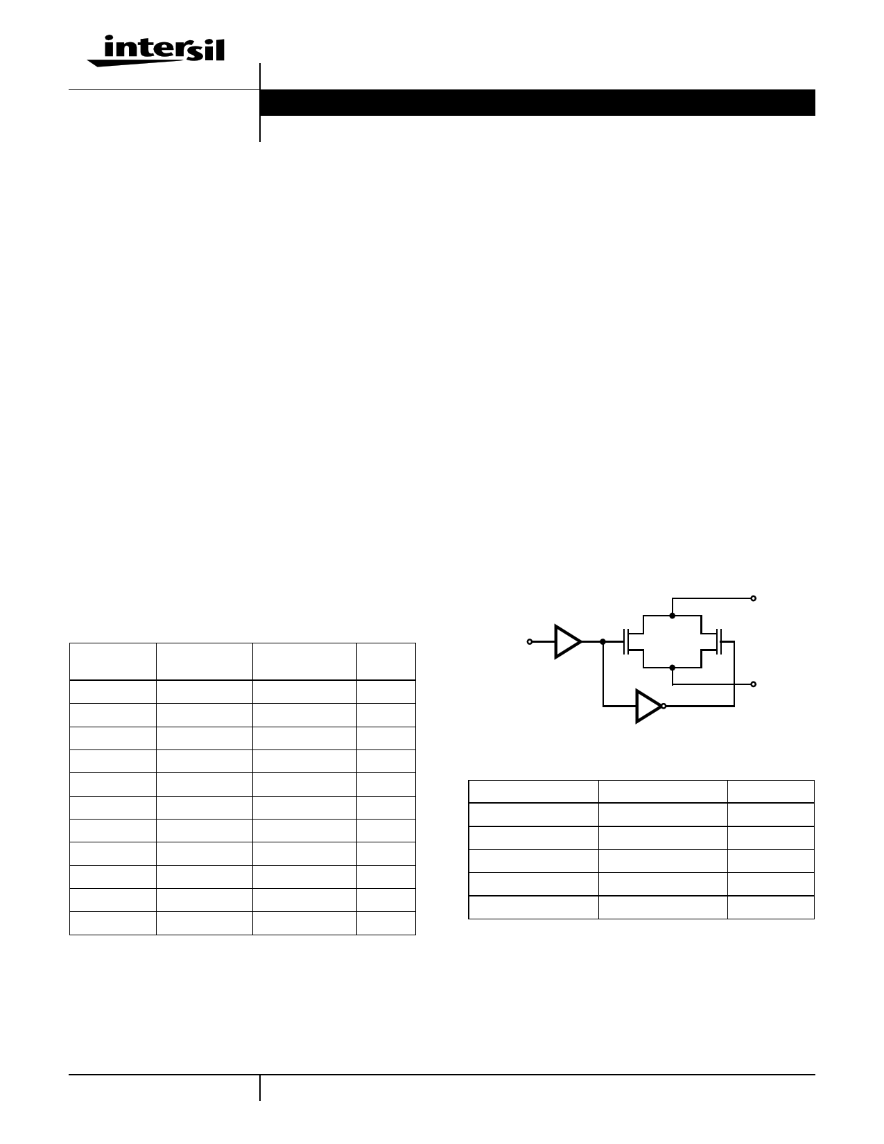
Functional Diagram
S
A NP
D
Functional Description
PART NUMBER
HI-5042
HI-5043
HI-5047
HI-5049
HI-5051
TYPE
SPDT
Dual SPDT
4PST
Dual DPST
Dual SPDT
rON
50Ω
50Ω
50Ω
25Ω
25Ω
1 CAUTION: These devices are sensitive to electrostatic discharge; follow proper IC Handling Procedures.
1-888-INTERSIL or 321-724-7143 | Intersil and Design is a trademark of Intersil Corporation. | Copyright © Intersil Corporation 2000
1 page 
HI-5042 thru HI-5051
Electrical Specifications
Supplies = +15V, -15V; VR = 0V; VAH (Logic Level High) = 2.4V, VAL (Logic Level Low) = 0.8V, VL = 5V,
Unless Otherwise Specified. For Test Conditions, Consult Performance Characteristics,
Unused Pins are Grounded (Continued)
PARAMETER
TEST
TEMP
-2
-5, -9
CONDITIONS
(oC)
MIN TYP MAX MIN TYP MAX UNITS
ON Leakage Current, ID(ON)
25
- 0.01 2
- 0.01 2
nA
Full - 2 200 - 2 200 nA
POWER REQUIREMENTS
Quiescent Power Dissipation, PD
I+, I-, IL, IR
I+, +15V Quiescent Current
(Note 5)
25
- 1.5 -
- 1.5 - mW
25 - - 0.2 - - 0.3 mA
Full - - 0.3 - - 0.5 mA
I-, -15V Quiescent Current
(Note 5)
Full - - 0.3 - - 0.5 mA
IL, +5V Quiescent Current
(Note 5)
IR, Ground Quiescent Current
(Note 5)
NOTES:
2. VOUT = ±10V, IOUT = 1mA.
3. VIN = 0V, CL = 10nF.
4. RL = 100Ω, f = 100kHz, VIN = 2.0VP-P, CL = 5pF.
5. VAL = 0V, VAH = 5V.
Full - - 0.3 - - 0.5 mA
Full - - 0.3 - - 0.5 mA
Test Circuits and Waveforms TA = 25oC, V+ = +15V, V- = -15V, VL = +5V, VR = 0V, VAH = 3V and VAL = 0.8V
Unless Otherwise Specified
1mA
V2
rON = 1mA
V2
IN OUT
±VIN
FIGURE 1A. TEST CIRCUIT
80
60
V+ = +12V
V+ = +10V
V- = -12V
40 V- = -10V
1.2
1.1
1.0
0.9
VIN = 0V
0.8
20 V+ = +15V
V- = -15V
0.7
0
-15 -10 -5
0
5 10
ANALOG SIGNAL LEVEL (V)
15
0.6
-50
-25
0 25 50 75
TEMPERATURE (oC)
100 125
FIGURE 1B. ON RESISTANCE vs ANALOG SIGNAL LEVEL
FIGURE 1C. NORMALIZED ON RESISTANCE vs TEMPERATURE
FIGURE 1. ON RESISTANCE
5
5 Page 
HI-5042 thru HI-5051
Ceramic Dual-In-Line Frit Seal Packages (CERDIP)
-A- -D-
E
-B-
bbb S C A - B S D S
c1 LEAD FINISH
BASE
METAL
(c)
b1
MM
(b)
SECTION A-A
BASE
PLANE
SEATING
PLANE
S1
b2
b
D
AA
e
Q
-C- A
L
eA/2
α
eA
c
ccc M C A - B S D S
aaa M C A - B S D S
NOTES:
1. Index area: A notch or a pin one identification mark shall be locat-
ed adjacent to pin one and shall be located within the shaded
area shown. The manufacturer’s identification shall not be used
as a pin one identification mark.
2. The maximum limits of lead dimensions b and c or M shall be
measured at the centroid of the finished lead surfaces, when
solder dip or tin plate lead finish is applied.
3. Dimensions b1 and c1 apply to lead base metal only. Dimension
M applies to lead plating and finish thickness.
4. Corner leads (1, N, N/2, and N/2+1) may be configured with a
partial lead paddle. For this configuration dimension b3 replaces
dimension b2.
5. This dimension allows for off-center lid, meniscus, and glass
overrun.
6. Dimension Q shall be measured from the seating plane to the
base plane.
7. Measure dimension S1 at all four corners.
8. N is the maximum number of terminal positions.
9. Dimensioning and tolerancing per ANSI Y14.5M - 1982.
10. Controlling dimension: INCH.
F16.3 MIL-STD-1835 GDIP1-T16 (D-2, CONFIGURATION A)
16 LEAD CERAMIC DUAL-IN-LINE FRIT SEAL PACKAGE
INCHES
MILLIMETERS
SYMBOL MIN MAX MIN MAX NOTES
A
- 0.200 - 5.08
-
b
0.014
0.026
0.36
0.66
2
b1
0.014
0.023
0.36
0.58
3
b2
0.045
0.065
1.14
1.65
-
b3
0.023
0.045
0.58
1.14
4
c
0.008
0.018
0.20
0.46
2
c1
0.008
0.015
0.20
0.38
3
D - 0.840 - 21.34 5
E
0.220
0.310
5.59
7.87
5
e 0.100 BSC
2.54 BSC
-
eA 0.300 BSC
7.62 BSC
-
eA/2
0.150 BSC
3.81 BSC
-
L
0.125
0.200
3.18
5.08
-
Q
0.015
0.060
0.38
1.52
6
S1 0.005 - 0.13 - 7
α
90o 105o 90o 105o
-
aaa
- 0.015 - 0.38
-
bbb
- 0.030 - 0.76
-
ccc
- 0.010 - 0.25
-
M
-
0.0015
-
0.038
2, 3
N 16
16 8
Rev. 0 4/94
All Intersil semiconductor products are manufactured, assembled and tested under ISO9000 quality systems certification.
Intersil semiconductor products are sold by description only. Intersil Corporation reserves the right to make changes in circuit design and/or specifications at any time with-
out notice. Accordingly, the reader is cautioned to verify that data sheets are current before placing orders. Information furnished by Intersil is believed to be accurate and
reliable. However, no responsibility is assumed by Intersil or its subsidiaries for its use; nor for any infringements of patents or other rights of third parties which may result
from its use. No license is granted by implication or otherwise under any patent or patent rights of Intersil or its subsidiaries.
For information regarding Intersil Corporation and its products, see web site www.intersil.com
Sales Office Headquarters
NORTH AMERICA
Intersil Corporation
P. O. Box 883, Mail Stop 53-204
Melbourne, FL 32902
TEL: (321) 724-7000
FAX: (321) 724-7240
EUROPE
Intersil SA
Mercure Center
100, Rue de la Fusee
1130 Brussels, Belgium
TEL: (32) 2.724.2111
FAX: (32) 2.724.22.05
ASIA
Intersil Ltd.
8F-2, 96, Sec. 1, Chien-kuo North,
Taipei, Taiwan 104
Republic of China
TEL: 886-2-2515-8508
FAX: 886-2-2515-8369
11
11 Page | ||
| Páginas | Total 11 Páginas | |
| PDF Descargar | [ Datasheet HI3-5043-5.PDF ] | |
Hoja de datos destacado
| Número de pieza | Descripción | Fabricantes |
| HI3-5043-5 | CMOS Analog Switches | Intersil |
| Número de pieza | Descripción | Fabricantes |
| SLA6805M | High Voltage 3 phase Motor Driver IC. |
Sanken |
| SDC1742 | 12- and 14-Bit Hybrid Synchro / Resolver-to-Digital Converters. |
Analog Devices |
|
DataSheet.es es una pagina web que funciona como un repositorio de manuales o hoja de datos de muchos de los productos más populares, |
| DataSheet.es | 2020 | Privacy Policy | Contacto | Buscar |