|
|
|
PDF MAX3866 Data sheet ( Hoja de datos )
| Número de pieza | MAX3866 | |
| Descripción | 2.5Gbps / +3.3V Combined Transimpedance/Limiting Amplifier | |
| Fabricantes | Maxim Integrated | |
| Logotipo | ||
Hay una vista previa y un enlace de descarga de MAX3866 (archivo pdf) en la parte inferior de esta página. Total 12 Páginas | ||
|
No Preview Available !
19-1433; Rev 1; 3/99
2.5Gbps, +3.3V Combined
Transimpedance/Limiting Amplifier
General Description
The MAX3866 combined transimpedance preamplifier
and limiting postamplifier is intended for application in
SDH/SONET systems operating at 2.488Gbps. It oper-
ates from a single +3.3V or +5V supply and provides a
differential output signal. The differential outputs are
each 50Ω reverse terminated (100Ω differential termi-
nation) for low-noise and high-speed signal perfor-
mance.
The small-signal bandwidth and noise performance is
specified for a source capacitance of 0.5pF. When the
MAX3866 is used with the PIN photodetector, sensitivi-
ties better than -22dBm can be achieved. The
MAX3866 is equipped with a programmable TTL loss-
of-power (LOP) output.
Features
o Input Sensitivities Better than -22dBm (7.8µAp-p)
o Overdrive Capability Better than +1.4dBm
(2.5mAp-p)
o Single +3.3V or +5V Supply
o 165mW Power Dissipation (at 3.3V)
o 1.8GHz Analog Input Bandwidth
o Programmable Loss-of-Power Indicator
o 100Ω Differential Output
Applications
SDH/SONET Transmission Systems
PIN/Preamplifier Receivers
2.488Gbps ATM Receivers
Regenerators for SDH/SONET
Ordering Information
PART
MAX3866E/D
TEMP. RANGE
(see Note)
PIN-PACKAGE
Dice
Note: Dice are designed to operate over a -40°C to +120°C
junction temperature (Tj) range, but are tested and guaranteed
at TA = +25°C.
Pad Configuration appears at end of data sheet.
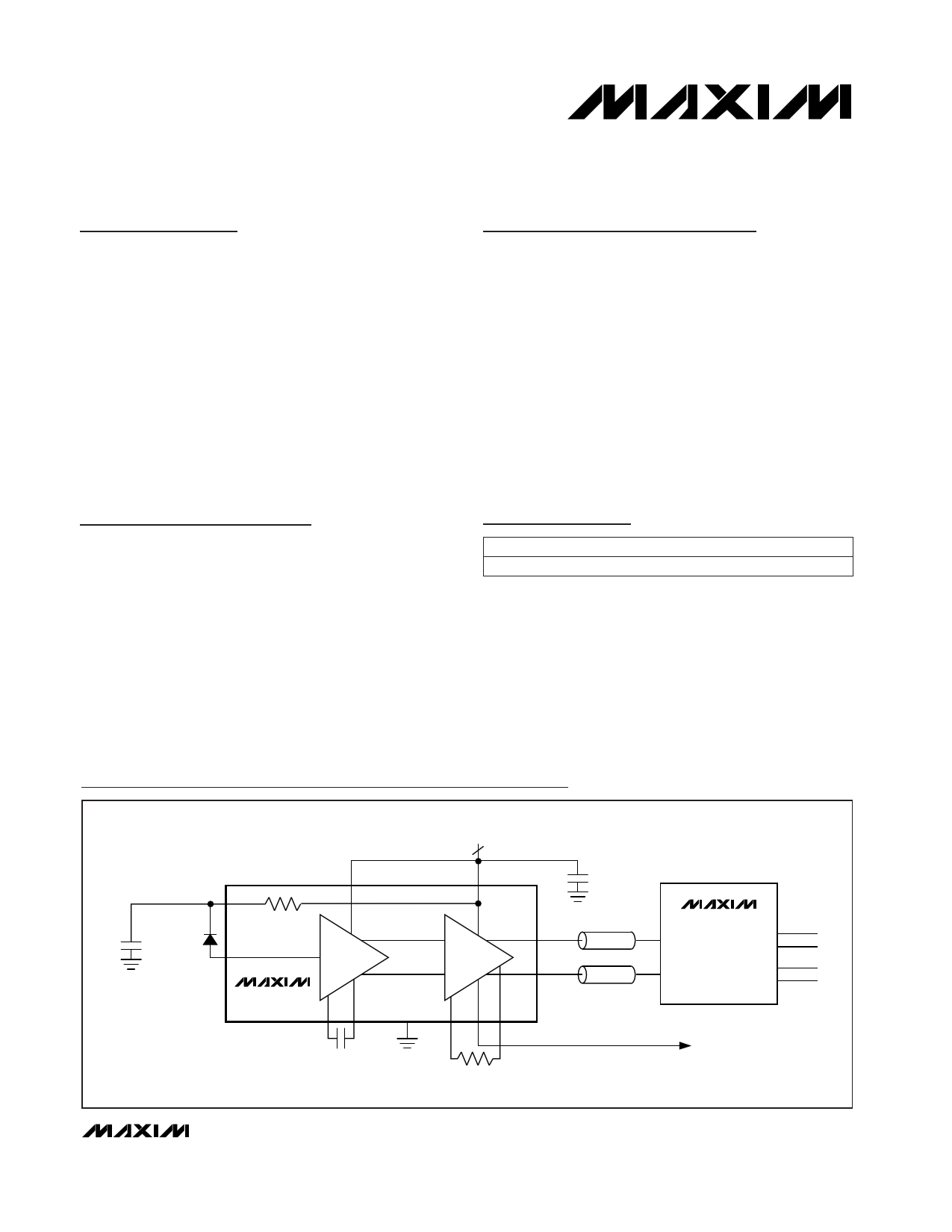
Typical Application Circuit
FIL
PHOTODIODE
IN+
VCCS
200Ω
PREAMP
MAX3866
CHF+
CHF-
CHF
+3.3V
VCCD
LIMITING
POSTAMP
OUT+ Zo = 50Ω
OUT-
Zo = 50Ω
PDC LOP
INV
RPD
MAX3875
CLOCK AND DATA
RECOVERY
________________________________________________________________ Maxim Integrated Products 1
For free samples & the latest literature: http://www.maxim-ic.com, or phone 1-800-998-8800.
For small orders, phone 1-800-835-8769.
1 page 
2.5Gbps, +3.3V Combined
Transimpedance/Limiting Amplifier
Typical Operating Circuits
CHF
100nF
3.3V
CHF-
VCCS
FIL
IN+
IN-
GND
CHF+
VCCD
LOP
MAX3866
OUT+
OUT-
PDC INV CPD- CPD+
RPD*
510Ω
10nF
100nF
OUT+
OUT-
100nF
CHF
100nF
5.0V
CHF-
VCCS
FIL
IN+
IN-
GND
CHF+
VCCD
LOP
MAX3866
OUT+
OUT-
PDC INV CPD- CPD+
RPD*
510Ω
100nF
OUT+
OUT-
100nF
3.3V OPERATION
* NOTE: IF LOP OPERATION IS NOT DESIRED, RPD = 0Ω
5.0V OPERATION
Circuit Description
Data Path
The combined preamplifier and limiting postamplifier
(Figure 1) accepts an input current from a photodiode
attached to the input pad IN+. The transimpedance
input amplifier stage converts the input current to an
output voltage with a typical transimpedance of 1.4kΩ.
The second stage of the data path is an active high-
pass filter. This filter converts the single-ended input
signal to a differential signal, eliminating the DC com-
ponent and adding approximately 16dB of gain. The
output of the highpass filter drives the power detector
and limiting amplifier circuitry.
The limiting amplifier circuit is the third stage of the
data signal path. It amplifies and limits the differential
input signal. The output stage is a differential pair with
internal 50Ω load resistors. The limited output voltage is
typically 145mVp-p.
Power Detector
The power detect circuit consists of an adjustable-gain
amplifier and combined rectifier with a lowpass filter.
The adjustable-gain amplifier is controlled by an op amp.
The gain is adjusted by means of an external resistor
connected between the PDC and INV pins.
The output voltage of the adjustable gain amplifier
drives the combined rectifier and lowpass filter circuit-
ry. The resulting DC voltage is fed to a Schmitt trigger,
which generates a high-level output signal if the DC
input signal is below the LOP assert level, thus causing
an LOP condition on the LOP output.
Design Procedure
Power Supply
The complete amplifier is supplied by a single supply
voltage, VCCD. For operation at 3.3V, the supply volt-
age is applied at both the VCCD and VCCS pins (see
Typical Operating Circuit). For operation at 5.0V, the
voltage is only applied at VCCD. In this case, VCCS is
on-chip controlled to approximately 3.2V. In the 5.0V
configuration, an external 10nF grounded capacitor is
required at the VCCS pin.
External Filter Capacitor CHF
The value of CHF affects the maximum speed at which
the compensation loop adjusts the input offset current.
CHF should be chosen between 10nF and 100nF. The
loop should be as slow as possible to reduce pattern-
dependent jitter. Maxim recommends a value of CHF =
100nF.
_______________________________________________________________________________________ 5
5 Page 
2.5Gbps, +3.3V Combined
Transimpedance/Limiting Amplifier
NOTES
______________________________________________________________________________________ 11
11 Page | ||
| Páginas | Total 12 Páginas | |
| PDF Descargar | [ Datasheet MAX3866.PDF ] | |
Hoja de datos destacado
| Número de pieza | Descripción | Fabricantes |
| MAX3861 | 2.7Gbps Post Amp with Automatic Gain Control | Maxim Integrated |
| MAX3863 | 2.7Gbps Laser Driver | Maxim Integrated Products |
| MAX3864 | 2.5Gbps / +3V to +5.5V / Wide Dynamic Range Transimpedance Preamplifier | Maxim Integrated |
| MAX3865 | 2.5Gbps Laser Driver with Automatic Modulation Control | Maxim Integrated |
| Número de pieza | Descripción | Fabricantes |
| SLA6805M | High Voltage 3 phase Motor Driver IC. |
Sanken |
| SDC1742 | 12- and 14-Bit Hybrid Synchro / Resolver-to-Digital Converters. |
Analog Devices |
|
DataSheet.es es una pagina web que funciona como un repositorio de manuales o hoja de datos de muchos de los productos más populares, |
| DataSheet.es | 2020 | Privacy Policy | Contacto | Buscar |