|
|
PDF MAX3391EEUD Data sheet ( Hoja de datos )
| Número de pieza | MAX3391EEUD | |
| Descripción | 15kV ESD-Protected / 1A / 16Mbps / Dual/Quad Low-Voltage Level Translators in UCSP | |
| Fabricantes | Maxim Integrated | |
| Logotipo |  |
|
Hay una vista previa y un enlace de descarga de MAX3391EEUD (archivo pdf) en la parte inferior de esta página. Total 25 Páginas | ||
|
No Preview Available !
19-2328; Rev 3; 9/03
±15kV ESD-Protected, 1µA, 16Mbps, Dual/Quad
Low-Voltage Level Translators in UCSP
General Description
The MAX3372E–MAX3379E and MAX3390E–MAX3393E
±15kV ESD-protected level translators provide the level
shifting necessary to allow data transfer in a multivoltage
system. Externally applied voltages, VCC and VL, set the
logic levels on either side of the device. A low-voltage
logic signal present on the VL side of the device appears
as a high-voltage logic signal on the VCC side of the
device, and vice-versa. The MAX3374E/MAX3375E/
MAX3376E/MAX3379E and MAX3390E–MAX3393E unidi-
rectional level translators level shift data in one direction
(VL → VCC or VCC → VL) on any single data line. The
MAX3372E/MAX3373E and MAX3377E/MAX3378E bidi-
rectional level translators utilize a transmission-gate-
based design (Figure 2) to allow data translation in either
direction (VL ↔ VCC) on any single data line. The
MAX3372E–MAX3379E and MAX3390E–MAX3393E
accept VL from +1.2V to +5.5V and VCC from +1.65V to
+5.5V, making them ideal for data transfer between low-
voltage ASICs/PLDs and higher voltage systems.
All devices in the MAX3372E–MAX3379E, MAX3390E–
MAX3393E family feature a three-state output mode that
reduces supply current to less than 1µA, thermal short-
circuit protection, and ±15kV ESD protection on the VCC
side for greater protection in applications that route sig-
nals externally. The MAX3372E/MAX3377E operate at a
guaranteed data rate of 230kbps. Slew-rate limiting
reduces EMI emissions in all 230kbps devices. The
MAX3373E–MAX3376E/MAX3378E/MAX3379E and
MAX3390E–MAX3393E operate at a guaranteed data rate
of 8Mbps over the entire specified operating voltage
range. Within specific voltage domains, higher data rates
are possible. (See Timing Characteristics.)
The MAX3372E–MAX3376E are dual level shifters
available in 3 x 3 UCSP™ and 8-pin SOT23-8 pack-
ages. The MAX3377E/MAX3378E/MAX3379E and
MAX3390E–MAX3393E are quad level shifters avail-
able in 3 x 4 UCSP and 14-pin TSSOP packages.
________________________Applications
SPI™, MICROWIRE™, and I2C™ Level
Translation
Low-Voltage ASIC Level Translation
Smart Card Readers
Cell-Phone Cradles
Portable POS Systems
Portable Communication Devices
Low-Cost Serial Interfaces
Cell Phones
GPS
Telecommunications Equipment
Features
o Guaranteed Data Rate Options
230kbps
8Mbps (+1.2V ≤ VL ≤ VCC ≤ +5.5V)
10Mbps (+1.2V ≤ VL ≤ VCC ≤ +3.3V)
16Mbps (+1.8V ≤ VL ≤ VCC ≤ +2.5V and +2.5V ≤
VL ≤ VCC ≤ +3.3V)
o Bidirectional Level Translation
(MAX3372E/MAX3373E and
MAX3377E/MAX3378E)
o Operation Down to +1.2V on VL
o ±15kV ESD Protection on I/O VCC Lines
o Ultra-Low 1µA Supply Current in Three-State
Output Mode
o Low-Quiescent Current (130µA typ)
o UCSP, SOT, and TSSOP Packages
o Thermal Short-Circuit Protection
Ordering Information
PART NUMBER
MAX3372EEKA-T
TEMP RANGE
-40°C to +85°C
PIN-
PACKAGE
8 SOT23-8
Ordering Information continued at end of data sheet.
Selector Guide appears at end of data sheet.
UCSP is a trademark of Maxim Integrated Products, Inc.
SPI is a trademark of Motorola, Inc.
I2C is a trademark of Phillips Corp.
MICROWIRE is a trademark of National Semiconductor Corp.
Pin Configurations
I/O VCC2 1
MAX3372E/
MAX3373E
GND 2
VL 3
I/O VL2 4
8 I/O VCC1
7 VCC
6 THREE-STATE
5 I/O VL1
SOT23-8
TOP VIEW
Pin Configurations continued at end of data sheet.
________________________________________________________________ Maxim Integrated Products 1
For pricing, delivery, and ordering information, please contact Maxim/Dallas Direct! at
1-888-629-4642, or visit Maxim’s website at www.maxim-ic.com.
1 page 
±15kV ESD-Protected, 1µA, 16Mbps, Dual/Quad
Low-Voltage Level Translators in UCSP
TIMING CHARACTERISTICS (continued)
(VCC = +1.65V to +5.5V, VL = +1.2V to (VCC + 0.3V), GND = 0, RLOAD = 1MΩ, I/O test signal of Figure 1, TA = TMIN to TMAX, unless
otherwise noted. Typical values are at VCC = +3.3V, VL = +1.8V, TA = +25°C, unless otherwise noted.) (Notes 1, 2)
PARAMETER
+1.2V ≤ VL ≤ VCC ≤ +3.3V
I/O VCC_ Rise Time (Note 4)
I/O VCC_ Fall Time (Note 5)
I/O VL_ Rise Time (Note 4)
I/O VL_ Fall Time (Note 5)
Propagation Delay
Channel-to-Channel Skew
Maximum Data Rate
+2.5V ≤ VL ≤ VCC ≤ +3.3V
I/O VCC_ Rise Time (Note 4)
I/O VCC_ Fall Time (Note 5)
I/O VL_ Rise Time (Note 4)
I/O VL_ Fall Time (Note 5)
Propagation Delay
Channel-to-Channel Skew
Maximum Data Rate
+1.8V ≤ VL ≤ VCC ≤ +2.5V
I/O VCC_ Rise Time (Note 4)
I/O VCC_ Fall Time (Note 5)
I/O VL_ Rise Time (Note 4)
I/O VL_ Fall Time (Note 5)
Propagation Delay
Channel-to-Channel Skew
Maximum Data Rate
SYMBOL
CONDITIONS
tRVCC
tFVCC
tRVL
tFVL
I/OVL-VCC
I/OVCC-VL
tSKEW
Driving I/O VL_
Driving I/O VCC_
Each translator equally loaded
tRVCC
tFVCC
tRVL
tFVL
I/OVL-VCC
I/OVCC-VL
tSKEW
Driving I/O VL_
Driving I/O VCC_
Each translator equally loaded
tRVCC
tFVCC
tRVL
tFVL
I/OVL-VCC
I/OVCC-VL
tSKEW
Driving I/O VL_
Driving I/O VCC_
Each translator equally loaded
MIN TYP MAX UNITS
25 ns
30 ns
30 ns
30 ns
20
ns
20
10 ns
10 Mbps
15 ns
15 ns
15 ns
15 ns
15
ns
15
10 ns
16 Mbps
15 ns
15 ns
15 ns
15 ns
15
ns
15
10 ns
16 Mbps
Note 1: All units are 100% production tested at TA = +25°C. Limits over the operating temperature range are guaranteed by design
and not production tested.
Note 2: For normal operation, ensure VL < (VCC + 0.3V). During power-up, VL > (VCC + 0.3V) will not damage the device.
Note 3: To ensure maximum ESD protection, place a 1µF capacitor between VCC and GND. See Applications Circuits.
Note 4: 10% to 90%
Note 5: 90% to 10%
_______________________________________________________________________________________ 5
5 Page 
±15kV ESD-Protected, 1µA, 16Mbps, Dual/Quad
Low-Voltage Level Translators in UCSP
circuitry limits the maximum data rate for devices in the
MAX3372E–MAX3379E, MAX3390E–MAX3393E family to
16Mbps. The maximum data rate also depends heavily
on the load capacitance (see Typical Operating
Characteristics), output impedance of the driver, and the
operational voltage range (see Timing Characteristics).
Speed-Up Circuitry
The MAX3373E–MAX3376E/MAX3378E/MAX3379E and
MAX3390E–MAX3393E feature a one-shot generator that
decreases the rise time of the output. When triggered,
MOSFETs PU1 and PU2 turn on for a short time to pull up
I/O VL_ and I/O VCC_ to their respective supplies (see
Figure 2b). This greatly reduces the rise time and propa-
gation delay for the low-to-high transition. The scope
photo of Rail-to-Rail Driving for 8Mbps Operation in the
Typical Operating Characteristics shows the speed-up
circuitry in operation.
Three-State Output Mode
Pull THREE-STATE low to place the MAX3372E–
MAX3379E and MAX3390E–MAX3393E in three-state out-
VL VCC
put mode. Connect THREE-STATE to VL (logic high) for
normal operation. Activating the three-state output mode
disconnects the internal 10kΩ pullup resistors on the I/O
VCC and I/O VL lines. This forces the I/O lines to a high-
impedance state, and decreases the supply current to
less than 1µA. The high-impedance I/O lines in three-
state output mode allow for use in a multidrop network.
When in three-state output mode, do not allow the voltage
at I/O VL_ to exceed (VL + 0.3V), or the voltage at I/O
VCC_ to exceed (VCC + 0.3V).
Thermal Short-Circuit Protection
Thermal overload detection protects the MAX3372E–
MAX3379E and MAX3390E–MAX3393E from short-circuit
fault conditions. In the event of a short-circuit fault, when
the junction temperature (TJ) reaches +152°C, a thermal
sensor signals the three-state output mode logic to force
the device into three-state output mode. When TJ has
cooled to +142°C, normal operation resumes.
VL VCC
VL VCC
VL VCC
MAX3372E–MAX3379E
AND MAX3390E–MAX3393E
I/O VL_
I/O VCC_
DATA
GND RLOAD
CLOAD
CLOAD
DATA
MAX3373E–MAX3376E,
MAX3378E/MAX3379E
AND MAX3390E–MAX3393E
I/O VL_
I/O VCC_
RLOAD
GND
I/O VL_
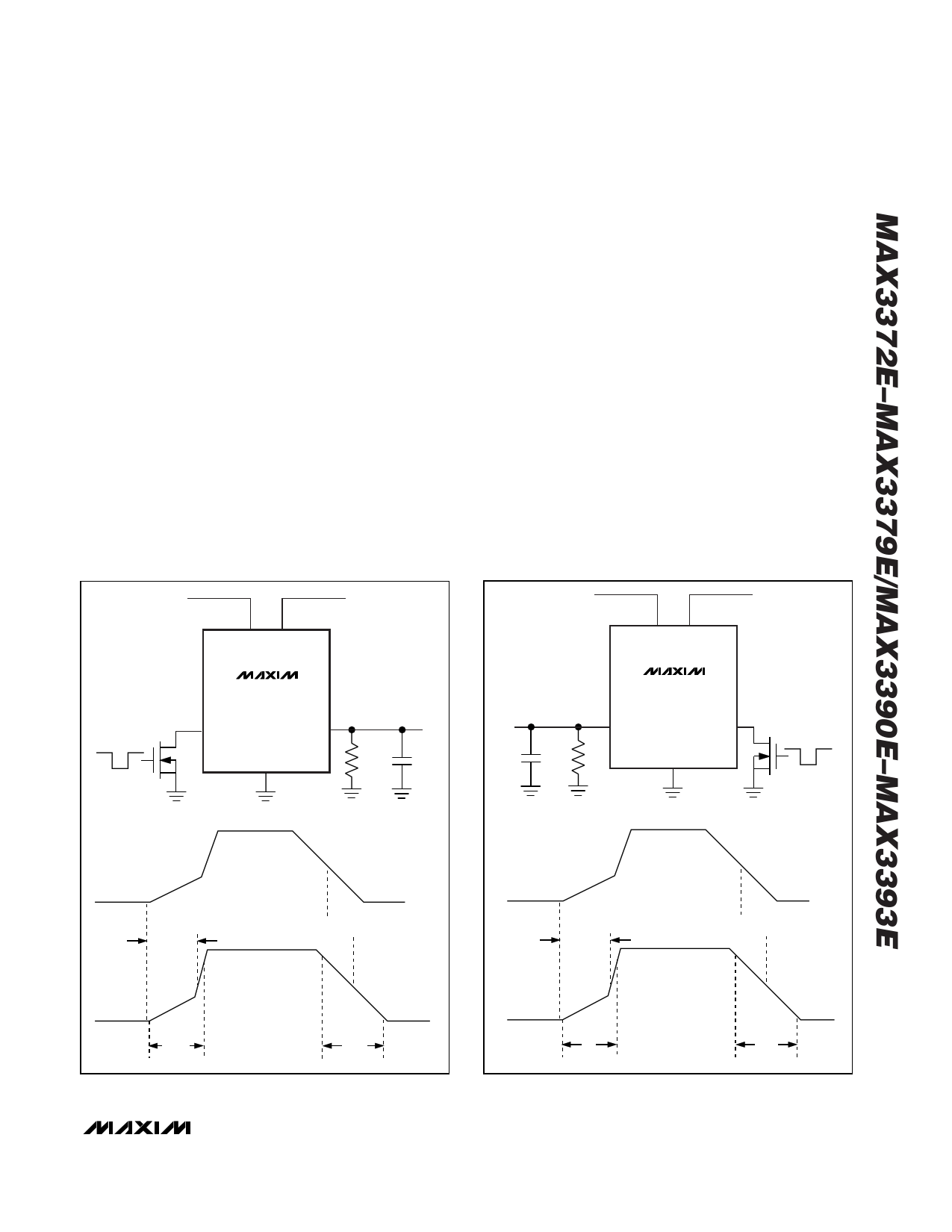
tPD-VCC-LH
tPD-VCC-HL
I/O VCC_
tPD-VL-LH
tPD-VL-HL
I/O VCC_
tRVCC
tFVCC
I/O VL_
tRVL
tFVL
Figure 1c. Open-Drain Driving I/O VCC
Figure 1d. Open-Drain Driving I/O VL
______________________________________________________________________________________ 11
11 Page | ||
| Páginas | Total 25 Páginas | |
| PDF Descargar | [ Datasheet MAX3391EEUD.PDF ] | |
Hoja de datos destacado
| Número de pieza | Descripción | Fabricantes |
| MAX3391EEUD | 15kV ESD-Protected / 1A / 16Mbps / Dual/Quad Low-Voltage Level Translators in UCSP | Maxim Integrated |
| Número de pieza | Descripción | Fabricantes |
| SLA6805M | High Voltage 3 phase Motor Driver IC. |
Sanken |
| SDC1742 | 12- and 14-Bit Hybrid Synchro / Resolver-to-Digital Converters. |
Analog Devices |
|
DataSheet.es es una pagina web que funciona como un repositorio de manuales o hoja de datos de muchos de los productos más populares, |
| DataSheet.es | 2020 | Privacy Policy | Contacto | Buscar |
