|
|
|
PDF 74F403A Data sheet ( Hoja de datos )
| Número de pieza | 74F403A | |
| Descripción | First-In First-Out (FIFO) Buffer Memory | |
| Fabricantes | Fairchild | |
| Logotipo | ||
Hay una vista previa y un enlace de descarga de 74F403A (archivo pdf) en la parte inferior de esta página. Total 15 Páginas | ||
|
No Preview Available !
www.DataSheet4U.com
January 1989
Revised May 1999
74F403A
First-In First-Out (FIFO) Buffer Memory
General Description
The 74F403A is an expandable fall-through type high-
speed First-In First-Out (FIFO) Buffer Memory optimized
for high-speed disk or tape controllers and communication
buffer applications. It is organized as 16-words by 4-bits
and may be expanded to any number of words or any num-
ber of bits in multiples of four. Data may be entered or
extracted asynchronously in serial or parallel, allowing eco-
nomical implementation of buffer memories.
The 74F403A has 3-STATE outputs which provide added
versatility and is fully compatible with all TTL families.
Features
s Serial or parallel input
s Serial or parallel output
s Expandable without external logic
s 3-STATE outputs
s Fully compatible with all TTL families
s Slim 24-pin package
s 9403A replacement
s Guaranteed 4000V minimum ESD protection
Ordering Code:
Order Number Package Number
Package Description
74F403ASPC
N24C
24-Lead Plastic Dual-In-Line Package (PDIP), JEDEC MS-100, 0.300 Wide
Devices also available in Tape and Reel. Specify by appending the suffix letter “X” to the ordering code.
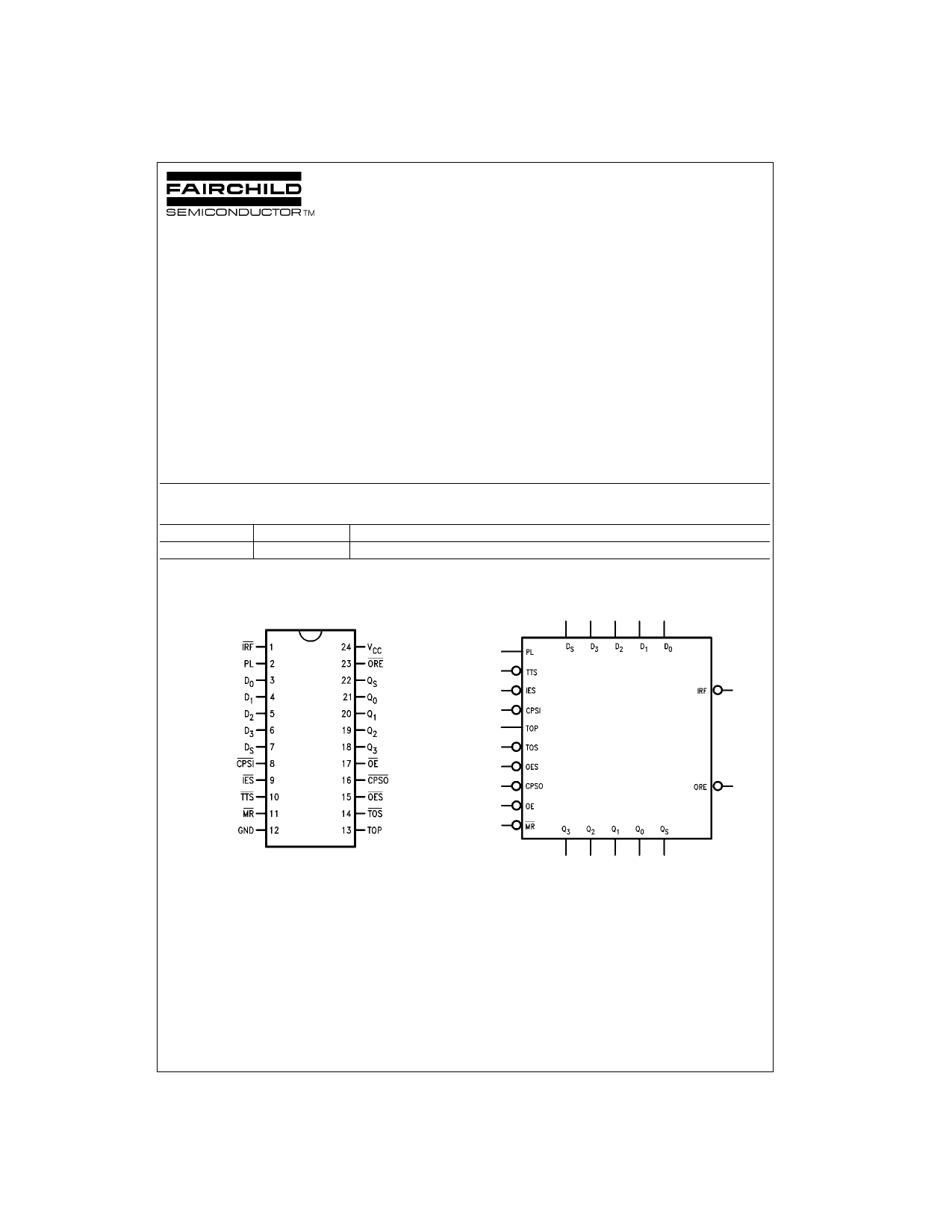
Connection Diagram
Logic Symbol
© 1999 Fairchild Semiconductor Corporation DS009536.prf
www.fairchildsemi.com
1 page 
EXPANSION
Vertical Expansion— The 74F403A may be vertically
expanded to store more words without external parts. The
interconnection is necessary to form a 46-word by 4-bit
FIFO are shown in Figure 4. Using the same technique,
and FIFO of (15n + 1)-words by 4-bits can be constructed,
where n is the number of devices. Note that expansion
does not sacrifice any of the 74F403A’s flexibility for serial/
parallel input and output.
FIGURE 4. A Vertical Expansion Scheme
Horizontal and Vertical Expansion— The 74F403A can
be expanded in both the horizontal and vertical directions
without any external parts and without sacrificing any of its
FIFO’s flexibility for serial/parallel input and output. The
interconnections necessary to form a 31-word by 16-bit
FIFO are shown in Figure 6. Using the same technique,
any FIFO of (15m + 1)-words by (4n)-bits can be con-
structed, where m is the number of devices in a column
and n is the number of devices in a row. Figure 7 and Fig-
ure 8 show the timing diagrams for serial data entry and
extraction for the 31-word by 16-bit FIFO shown in Figure
6. The final position of data after serial insertion of 496 bits
into the FIFO array of Figure 6 is shown in Figure 9.
Interlocking Circuitry— Most conventional FIFO designs
provide status signals analogous to IRF and ORE. How-
ever, when these devices are operated in arrays, variations
in unit to unit operating speed require external gating to
assure all devices have completed an operation. The
74F403A incorporates simple but effective “master/slave”
interlocking circuitry to eliminate the need for external gat-
ing.
In the 74F403A array of Figure 6 devices 1 and 5 are
defined as “row masters” and the other devices are slaves
to the master in their row. No slave in a given row will initial-
ize its Input Register until it has received LOW on its IES
input from a row master or a slave of higher priority.
In a similar fashion, the ORE outputs of slaves will not go
HIGH until their OES inputs have gone HIGH.This inter-
locking scheme ensures that new input data may be
accepted by the array when the IRF output of the final
slave in that row goes HIGH and that output data for the
array may be extracted when the ORE of the final slave in
the output row goes HIGH.
The row master is established by connecting its IES input
to ground while a slave receives its IES input from the IRF
output of the next higher priority device. When an array of
74F403A FIFOs is initialized with a LOW on the MR inputs
of all devices, the IRF outputs of all devices will be HIGH.
Thus, only the row master receives a LOW on the IES input
during initialization. Figure 10 is a conceptual logic diagram
of the internal circuitry which determines master/slave
operation. Whenever MR and IES are LOW, the Master
Latch is set. Whenever TTS goes LOW the Request Initial-
ization Flip-Flop will be set. If the Master Latch is HIGH, the
Input Register will be immediately initialized and the
Request Initialization Flip-Flop reset. If the Master Latch is
reset, the Input Register is not initialized until IES goes
LOW. In array operation, activating the TTS initiates a rip-
ple input register initialization from the row master to the
last slave.
A similar operation takes place for the output register.
Either a TOS or TOP input initiates a load-from-stack oper-
ation and sets the ORE Request Flip-Flop. If the Master
Latch is set, the last Output Register Flip-Flop is set and
ORE goes HIGH. If the Master Latch is reset, the ORE out-
put will be LOW until an OES input is received.
5 www.fairchildsemi.com
5 Page 
AC Electrical Characteristics (Continued)
Symbol
Parameter
tPZH
Turn On Time
tPZL TOS to QS
tDFT Fall Through Time
tAP Parallel Appearance Time,
ORE to Q0-Q3
tAS Serial Appearance Time,
ORE to QS
AC Operating Requirements
Symbol
Parameter
tS(H)
tS(L)
tH(H)
tH(L)
tS(L)
tS(L)
tS(L)
tS(L)
tS(H)
tS(L)
tH(H)
tH(L)
tW(H)
tW(L)
tW(H)
tW(L)
Set-up Time HIGH or LOW
DS to Negative CPSI
Hold Time, HIGH or LOW
DS to CPSI
Set-up Time, LOW
TTS to IRF
Serial or Parallel Mode
Set-up Time, LOW
Negative-Going ORE to
Negative-Going TOS
Set-up Time, LOW
Negative-Going IES to CPSI
Set-up Time, LOW
Negative-Going TTS to CPSI
Set-up Time, HIGH or LOW
Parallel Inputs to PL
Hold Time, HIGH or LOW
Parallel Inputs to PL
CPSI Pulse Width
HIGH or LOW
PL Pulse Width, HIGH
TTS Pulse Width, LOW
Serial or Parallel Mode
TA = +25°C
VCC = +5.0V
CL = 50 pF
Min Max
8.5 21.0
8.5 20.0
45.0
80.0
−10.0
−1.0
−10.0
2.0
TA = +25°C
VCC = +5.0V
Min Max
1.0
1.0
3.5
3.5
0
0
3.0
14.0
0
0
2.0
2.0
5.0
3.0
4.0
3.5
tW(L)
tW(H)
tW(L)
tW(H)
tW(L)
tREC
MR Pulse Width, LOW
TOP Pulse Width
HIGH or LOW
CPSO Pulse Width
HIGH or LOW
Recovery Time
MR to Any Input
3.5
4.5
3.5
4.5
3.0
5.0
TA = 0° to +70°C
VCC = +5.0V
CL = 50 pF
Min Max
8.0 24.0
8.0 21.0
35.0
95.0
−10.0
−1.0
−10.0
20
Units
Figure
Number
ns
ns Figure 16
ns
TA = 0°C to +70°C
VCC = +5.0V
Min Max
1.0
1.0
3.5
3.5
0
0
4.0
15.5
0
0
2.5
2.5
6.0
5.0
5.0
4.0
4.0
5.5
4.0
5.5
4.0
5.5
Units
Figure
Number
ns
Figure 11
Figure 12
Figure 11
ns
Figure 12
Figure 17
Figure 18
ns
Figure 13
Figure 14
ns Figure 12
ns Figure 12
ns
ns
Figure 11
Figure 12
ns
Figure 17
Figure 18
Figure 11
ns
Figure 12
Figure 13
Figure 14
ns Figure 16
ns Figure 15
ns
Figure 13
Figure 14
ns Figure 16
11 www.fairchildsemi.com
11 Page | ||
| Páginas | Total 15 Páginas | |
| PDF Descargar | [ Datasheet 74F403A.PDF ] | |
Hoja de datos destacado
| Número de pieza | Descripción | Fabricantes |
| 74F403 | First-In First-Out (FIFO) Buffer Memory | Fairchild |
| 74F403A | First-In First-Out (FIFO) Buffer Memory | Fairchild |
| 74F403ASPC | First-In First-Out (FIFO) Buffer Memory | Fairchild |
| Número de pieza | Descripción | Fabricantes |
| SLA6805M | High Voltage 3 phase Motor Driver IC. |
Sanken |
| SDC1742 | 12- and 14-Bit Hybrid Synchro / Resolver-to-Digital Converters. |
Analog Devices |
|
DataSheet.es es una pagina web que funciona como un repositorio de manuales o hoja de datos de muchos de los productos más populares, |
| DataSheet.es | 2020 | Privacy Policy | Contacto | Buscar |