|
|
|
PDF LM2940 Data sheet ( Hoja de datos )
| Número de pieza | LM2940 | |
| Descripción | 1A Low Dropout Regulator | |
| Fabricantes | National Semiconductor | |
| Logotipo | ||
Hay una vista previa y un enlace de descarga de LM2940 (archivo pdf) en la parte inferior de esta página. Total 17 Páginas | ||
|
No Preview Available !
March 2000
LM2940/LM2940C
1A Low Dropout Regulator
General Description
The LM2940/LM2940C positive voltage regulator features
the ability to source 1A of output current with a dropout volt-
age of typically 0.5V and a maximum of 1V over the entire
temperature range. Furthermore, a quiescent current reduc-
tion circuit has been included which reduces the ground cur-
rent when the differential between the input voltage and the
output voltage exceeds approximately 3V. The quiescent
current with 1A of output current and an input-output differ-
ential of 5V is therefore only 30 mA. Higher quiescent cur-
rents only exist when the regulator is in the dropout mode
(VIN − VOUT ≤ 3V).
Designed also for vehicular applications, the LM2940/
LM2940C and all regulated circuitry are protected from re-
verse battery installations or 2-battery jumps. During line
transients, such as load dump when the input voltage can
momentarily exceed the specified maximum operating volt-
age, the regulator will automatically shut down to protect
both the internal circuits and the load. The LM2940/
LM2940C cannot be harmed by temporary mirror-image in-
sertion. Familiar regulator features such as short circuit and
thermal overload protection are also provided.
Features
n Dropout voltage typically 0.5V @IO = 1A
n Output current in excess of 1A
n Output voltage trimmed before assembly
n Reverse battery protection
n Internal short circuit current limit
n Mirror image insertion protection
n P+ Product Enhancement tested
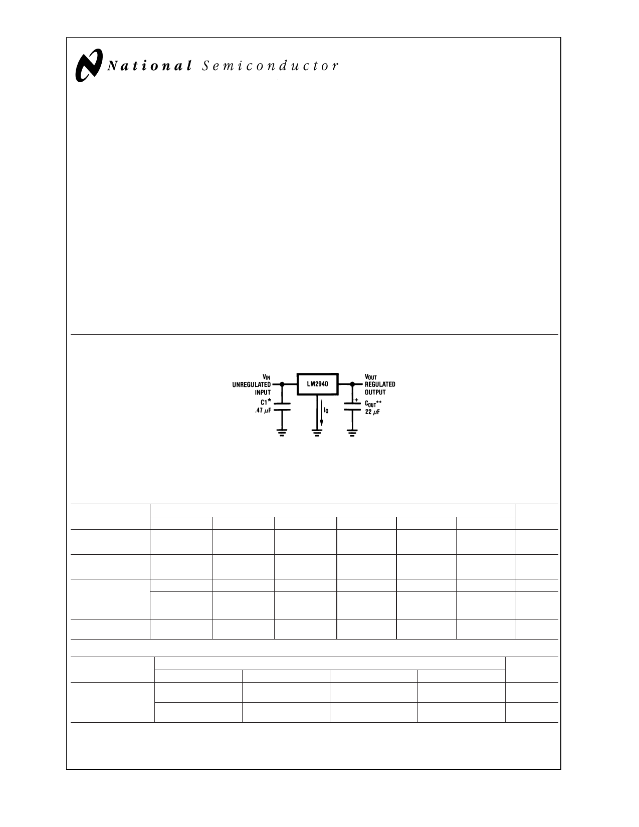
Typical Application
DS008822-3
*Required if regulator is located far from power supply filter.
**COUT must be at least 22 µF to maintain stability. May be increased without bound to maintain regulation during transients. Locate as close as possible
to the regulator. This capacitor must be rated over the same operating temperature range as the regulator and the ESR is critical; see curve.
Ordering Information
Temperature
Range
0˚C ≤ TJ ≤ 125˚C
−40˚C ≤ TJ ≤ 125˚C
−40˚C ≤ TJ ≤ 85˚C
SOT-223 Package
Marking
Output Voltage
Package
5.0 8.0 9.0 10 12 15
LM2940CT-5.0
LM2940CT-9.0
LM2940CT-12 LM2940CT-15 TO-220
LM2940CS-5.0
LM2940CS-9.0
LM2940CS-12 LM2940CS-15 TO-263
LM2940T-5.0 LM2940T-8.0 LM2940T-9.0 LM2940T-10 LM2940T-12
TO-220
LM2940S-5.0 LM2940S-8.0 LM2940S-9.0 LM2940S-10 LM2940S-12
TO-263
LM2940IMP-5.0 LM2940IMP-8.0 LM2940IMP-9.0 LM2940IMP-10 LM2940IMP-12 LM2940IMP-15 SOT-223
LM2940IMPX-5.0 LM2940IMPX-8.0 LM2940IMPX-9.0 LM2940IMPX-10 LM2940IMPX-12 LM2940IMPX-15 SOT-223
in Tape
and Reel
L53B
L54B
L0EB
L55B
L56B
L70B
The physical size of the SOT-223 is too small to contain the full device part number. The package markings indicated are what will appear on the actual device.
Temperature
Range
−55˚C ≤ TJ ≤ 125˚C
5.0
LM2940J-5.0/883
5962-8958701EA
LM2940WG5.0/883
5962-8958701XA
Output Voltage
8.0 12
LM2940J-8.0/883
5962-9088301QEA
LM2940J-12/883
5962-9088401QEA
15
LM2940J-15/883
5962-9088501QEA
Package
J16A
WG16A
For information on military temperature range products, please go to the Mil/Aero Web Site at http://www.national.com/appinfo/milaero/index.html.
© 2000 National Semiconductor Corporation DS008822
www.national.com
1 page 
Electrical Characteristics (Continued)
VIN = VO + 5V, IO = 1A, CO = 22 µF, unless otherwise specified. Boldface limits apply over the entire operating tempera-
ture range of the indicated device. All other specifications apply for TA = TJ = 25˚C.
Output Voltage (VO)
Parameter
Conditions
9V
LM2940
Typ Limit
10V
LM2940
Typ Limit
Units
(Note 4)
(Note 4)
Short Circuit
Current
(Note 6)
1.9 1.6
1.9
1.6
AMIN
Maximum Line
Transient
RO = 100Ω
T ≤ 100 ms
LM2940
LM2940C
75 60/60
55 45
75
60/60
VMIN
Reverse Polarity
DC Input Voltage
RO = 100Ω
LM2940
LM2940C
−30 −15/−15
−30 −15
−30
−15/−15
VMIN
Reverse Polarity
Transient Input
RO = 100Ω
T ≤ 100 ms
Voltage
LM2940
LM2940C
−75 −50/−50
−55 −45/−45
−75
−50/−50
VMIN
Electrical Characteristics
VIN = VO + 5V, IO = 1A, CO = 22 µF, unless otherwise specified. Boldface limits apply over the entire operating tempera-
ture range of the indicated device. All other specifications apply for TA = TJ = 25˚C.
Output Voltage (VO)
Parameter
Conditions
12V 15V
LM2940 LM2940/833
LM2940 LM2940/833
Units
Typ Limit
Limit Typ Limit
Limit
(Note 4)
(Note 5)
(Note 4)
(Note 5)
Output Voltage
Line Regulation
Load Regulation
5 mA ≤ IO ≤1A
VO + 2V ≤ VIN ≤ 26V,
IO = 5 mA
50 mA ≤ IO ≤ 1A
LM2940, LM2940/883
LM2940C
12.00
20
13.6V ≤ VIN ≤ 26V
11.64/11.40 11.64/11.40
12.36/12.60 12.36/12.60
120 75/120
15.00
20
16.75V ≤ VIN ≤ 26V
14.55/14.25 14.55/14.25
15.45/15.75 15.45/15.75
150 95/150
VMIN
VMAX
mVMAX
55 120/200
55 120
120/190
70
150
150/240 mVMAX
Output
100 mADC and
Impedance
20 mArms,
80
1000/1000 100
1000/1000 mΩ
Quiescent
Current
fO = 120 Hz
VO +2V ≤ VIN ≤ 26V,
IO = 5 mA
LM2940, LM2940/883
LM2940C
10
10
15/20
15
15/20
10
15
15/20
mAMAX
Output Noise
Voltage
Ripple Rejection
VIN = VO + 5V, IO = 1A
10 Hz − 100 kHz,
IO = 5 mA
fO = 120 Hz, 1 Vrms,
IO = 100 mA
LM2940
LM2940C
30
360
66
66
45/60
54/48
54
50/60
1000/1000
30
450
64
45/60
52
50/60
1000/1000
mAMAX
µVrms
dBMIN
fO = 1 kHz, 1 Vrms,
IO = 5 mA
52/46
48/42
dBMIN
5 www.national.com
5 Page 
Application Hints (Continued)
an aluminum electrolytic with a solid Tantalum, with the total
capacitance split about 75/25% with the Aluminum being the
larger value.
If two capacitors are paralleled, the effective ESR is the par-
allel of the two individual values. The “flatter” ESR of the Tan-
talum will keep the effective ESR from rising as quickly at low
temperatures.
HEATSINKING
A heatsink may be required depending on the maximum
power dissipation and maximum ambient temperature of the
application. Under all possible operating conditions, the junc-
tion temperature must be within the range specified under
Absolute Maximum Ratings.
To determine if a heatsink is required, the power dissipated
by the regulator, PD, must be calculated.
The figure below shows the voltages and currents which are
present in the circuit, as well as the formula for calculating
the power dissipated in the regulator:
DS008822-37
IIN = IL ÷ IG
PD = (VIN − VOUT) IL + (VIN) IG
FIGURE 2. Power Dissipation Diagram
The next parameter which must be calculated is the maxi-
mum allowable temperature rise, TR (max). This is calcu-
lated by using the formula:
TR (max) = TJ(max) − TA (max)
where: TJ (max) is the maximum allowable junction tem-
perature, which is 125˚C for commercial
grade parts.
TA (max) is the maximum ambient temperature
which will be encountered in the applica-
tion.
Using the calculated values for TR(max) and PD, the maxi-
mum allowable value for the junction-to-ambient thermal re-
sistance, θ(J−A), can now be found:
θ(J−A) = TR (max)/PD
IMPORTANT: If the maximum allowable value for θ(J−A) is
found to be ≥ 53˚C/W for the TO-220 package, ≥ 80˚C/W for
the TO-263 package, or ≥174˚C/W for the SOT-223 pack-
age, no heatsink is needed since the package alone will dis-
sipate enough heat to satisfy these requirements.
If the calculated value for θ(J−A)falls below these limits, a
heatsink is required.
HEATSINKING TO-220 PACKAGE PARTS
The TO-220 can be attached to a typical heatsink, or se-
cured to a copper plane on a PC board. If a copper plane is
to be used, the values of θ(J−A) will be the same as shown in
the next section for the TO-263.
If a manufactured heatsink is to be selected, the value of
heatsink-to-ambient thermal resistance, θ(H−A), must first be
calculated:
θ(H−A) = θ(J−A) − θ(C−H) − θ(J−C)
Where: θ(J−C) is defined as the thermal resistance from
the junction to the surface of the case. A
value of 3˚C/W can be assumed for θ(J−C)
for this calculation.
θ(C−H) is defined as the thermal resistance be-
tween the case and the surface of the heat-
sink. The value of θ(C−H) will vary from
about 1.5˚C/W to about 2.5˚C/W (depend-
ing on method of attachment, insulator,
etc.). If the exact value is unknown, 2˚C/W
should be assumed for θ(C−H).
When a value for θ(H−A) is found using the equation shown,
a heatsink must be selected that has a value that is less than
or equal to this number.
θ(H−A) is specified numerically by the heatsink manufacturer
in the catalog, or shown in a curve that plots temperature rise
vs power dissipation for the heatsink.
HEATSINKING TO-263 AND SOT-223 PACKAGE PARTS
Both the TO-263 (“S”) and SOT-223 (“MP”) packages use a
copper plane on the PCB and the PCB itself as a heatsink.
To optimize the heat sinking ability of the plane and PCB,
solder the tab of the package to the plane.
Figure 3 shows for the TO-263 the measured values of θ(J−A)
for different copper area sizes using a typical PCB with 1
ounce copper and no solder mask over the copper area used
for heatsinking.
DS008822-38
FIGURE 3. θ(J−A) vs Copper (1 ounce) Area for the
TO-263 Package
As shown in the figure, increasing the copper area beyond 1
square inch produces very little improvement. It should also
be observed that the minimum value of θ(J−A) for the TO-263
package mounted to a PCB is 32˚C/W.
As a design aid, Figure 4 shows the maximum allowable
power dissipation compared to ambient temperature for the
TO-263 device (assuming θ(J−A) is 35˚C/W and the maxi-
mum junction temperature is 125˚C).
11 www.national.com
11 Page | ||
| Páginas | Total 17 Páginas | |
| PDF Descargar | [ Datasheet LM2940.PDF ] | |
Hoja de datos destacado
| Número de pieza | Descripción | Fabricantes |
| LM2940 | 1A Low Dropout Regulator | National Semiconductor |
| LM2940 | 1-A LOW-DROPOUT VOLTAGE REGULATOR | Texas |
| LM2940 | 1A LOW-DROPOUT POSITIVE VOLTAGE REGULATOR | Unisonic Technologies |
| LM2940-N | LM2940x 1-A Low Dropout Regulator (Rev. J) | Texas Instruments |
| Número de pieza | Descripción | Fabricantes |
| SLA6805M | High Voltage 3 phase Motor Driver IC. |
Sanken |
| SDC1742 | 12- and 14-Bit Hybrid Synchro / Resolver-to-Digital Converters. |
Analog Devices |
|
DataSheet.es es una pagina web que funciona como un repositorio de manuales o hoja de datos de muchos de los productos más populares, |
| DataSheet.es | 2020 | Privacy Policy | Contacto | Buscar |