|
|
|
PDF OPA655 Data sheet ( Hoja de datos )
| Número de pieza | OPA655 | |
| Descripción | Wideband / Unity Gain Stable / FET-Input OPERATIONAL AMPLIFIER | |
| Fabricantes | Burr-Brown | |
| Logotipo | ||
Hay una vista previa y un enlace de descarga de OPA655 (archivo pdf) en la parte inferior de esta página. Total 14 Páginas | ||
|
No Preview Available !
® OPA655
OPA655
OPA655
Wideband, Unity Gain Stable, FET-Input
OPERATIONAL AMPLIFIER
FEATURES
q 400MHz UNITY GAIN BANDWIDTH
q LOW INPUT BIAS CURRENT: 5pA
q HIGH INPUT IMPEDANCE: 1012Ω || 1.0pF
q ULTRA-LOW dG/dP: 0.006%/0.009°
q LOW DISTORTION: 90dB SFDR at 5MHz
q FAST SETTLING: 17ns (0.01%)
q HIGH OUTPUT CURRENT: 60mA
q FAST OVERDRIVE RECOVERY
APPLICATIONS
q WIDEBAND PHOTODIODE
AMPLIFIER
q PEAK DETECTOR
q CCD OUTPUT BUFFER
q ADC INPUT BUFFER
q HIGH SPEED INTEGRATOR
q TEST AND MEASUREMENT FRONT END
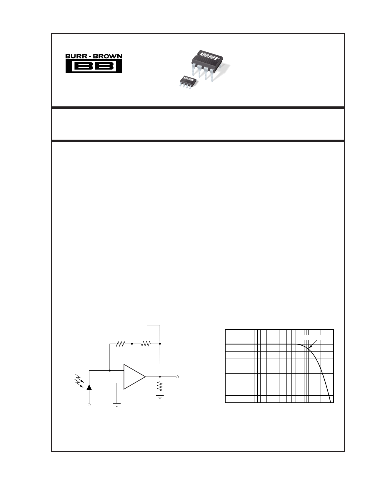
1pF
499kΩ
499kΩ
λ OPA655
(47pF)
100Ω
VO
–Vb
Wideband Photodiode Transimpedance Amplifier
DESCRIPTION
The OPA655 combines a very wideband, unity gain
stable, voltage feedback op amp with a FET input
stage to offer an ultra high dynamic range amplifier
for ADC buffering and transimpedance applications.
Extremely low harmonic distortion along with excel-
lent pulse settling characteristics will support even the
most demanding ADC input buffer requirements.
The broad unity gain stable bandwidth and FET input
allows exceptional performance in high speed, low
noise integrators.
The high input impedance and low bias current pro-
vided by the FET input is further supported by the
ultra-low 6nV/√Hz input voltage noise to achieve a
very low integrated noise in wideband photodiode
transimpedance applications.
Broad transimpedance bandwidths are achievable given
the OPA655’s high 240MHz gain bandwidth product.
As shown below, a –3dB bandwidth of 1MHz is
provided even for a high 1MΩ transimpedance gain
from a 47pF source capacitance.
1MΩ TRANSIMPEDANCE BANDWIDTH
130
1MHz Bandwidth
120
110
100
90
80
10kHz
100kHz
Frequency
1MHz
5MHz
International Airport Industrial Park • Mailing Address: PO Box 11400, Tucson, AZ 85734 • Street Address: 6730 S. Tucson Blvd., Tucson, AZ 85706 • Tel: (520) 746-1111 • Twx: 910-952-1111
Internet: http://www.burr-brown.com/ • FAXLine: (800) 548-6133 (US/Canada Only) • Cable: BBRCORP • Telex: 066-6491 • FAX: (520) 889-1510 • Immediate Product Info: (800) 548-6132
© 1994 Burr-Brown Corporation
PDS-1271D
Printed in U.S.A. May, 1997
1 page 
TYPICAL PERFORMANCE CURVES (CONT)
At TA = +25°C, VS = ±5V, RFB = 100Ω, and RL = 100Ω, unless otherwise noted. RFB = 0 for G = +1.
–40
–50
–60
–70
–80
–90
–100
1M
HARMONIC DISTORTION vs FREQUENCY
(VO = 2Vp-p, G = +1)
2fO
3fO
10M
Frequency (Hz)
100M
HARMONIC DISTORTION vs FREQUENCY
(VO = 2Vp-p, G = +2)
–40
–50
–60
–70
–80
–90
–100
1M
2fO
3fO
10M
Frequency (Hz)
100M
–40
–50
–60
–70
–80
–90
–100
1M
HARMONIC DISTORTION vs FREQUENCY
(VO = 2Vp-p, G = +5)
2fO
3fO
10M
Frequency (Hz)
100M
–85
–90
–95
–100
–105
–110
–115
0.1
5MHz HARMONIC DISTORTION
vs OUTPUT SWING
G = +1
2fO
3fO
1
Output Swing (Vp-p)
10
–60
–65
–70
–75
–80
–85
–90
–95
0.1
10MHz HARMONIC DISTORTION
vs OUTPUT SWING
G = +1
2fO
3fO
1
Output Swing (Vp-p)
10
HARMONIC DISTORTION vs TEMPERATURE
(VO = 2Vp-p, G = +1, fO = 5MHz)
–85
–90
2fO
–95
3fO
–100
–50
–25
0 25 50
Temperature (°C)
75 100
®
5 OPA655
5 Page 
BANDWIDTH vs RF
30
CD = 10pF
CD = 20pF
10
CD =50pF
1
0.3
10
CD = 100pF
CD = 200pF
100
Transimpedance Gain, RF (kΩ)
FIGURE 8. Maximally Flat Bandwidth.
1000
HIGH SPEED INSTRUMENTATION
DIFFERENTIAL AMPLIFIER
Very high speed differential amplifiers can be implemented
using the OPA655. The very low input bias currents allow
relatively high resistor values to be used in a standard single
op amp differential configuration. Alternatively, a very high
input impedance differential amplifier can be implemented
using a three op amp instrumentation amplifier topology as
shown in Figure 9.
V–
300Ω
300Ω
OPA655
RF
100Ω
CT
1.5 to 6pF
RG
100Ω
RF
100Ω
OPA651
50Ω
50Ω
Load
300Ω
300Ω
OPA655
V+
FIGURE 9. High Input Impedance, Broadband INA.
In this example, the OPA655’s provide a differential gain of:
1
+
2RF
RG
=
3
and a common mode gain of 1 to the input of the OPA651
differential stage. The OPA651, a gain of 2 stable, broad-
band voltage feedback op amp, rejects the common mode
signal and provides a differential gain of 1/2 the matched
50Ω load. This circuit delivers a 136MHz bandwidth at a
differential gain of 1.5V/V (3.5dB) to the matched load as
shown in Figure 10. The CT tuning capacitor is used to
match the high frequency gains for the two signal paths to
improve the high frequency CMRR. Using this adjustment,
a CMRR > 40dB through 100MHz was achieved.
DIFFERENTIAL INPUT
3.5dB
2.5
1.5
.5
136MHz
1M
10M
100M
1G
FIGURE 10. Measured Frequency Response for INA.
OPTIMIZING PERFORMANCE
DC ACCURACY
The OPA655 is laser trimmed for low input offset voltage,
limiting the need for external trim circuits. In most cases, the
low bias current of the FET input will not contribute signifi-
cantly to the output DC error. For example, at minimum gain
(G = +1) and maximum temperature (85°C), the error
contribution due to the inverting input bias current would
only exceed the input offset voltage for feedback resistors >
(1mV/3.2nA) = 312kΩ. Only for relatively high source and/
or feedback resistor values will the input bias current con-
tribute significantly to the output DC error. Similarly, since
the two input bias currents are very low, but not tightly
matched, input bias current cancellation through source
impedance matching is not recommended.
Changes in the power supply voltages contribute to shifts
in the input offset voltage. This can be calculated using
the PSR specifications. For example, a 0.5V change in
the negative power supply will show up typically as a
0.5V • 10(–65/20) = 0.28mV change in the input offset voltage.
Negative common mode voltage inputs can cause an in-
crease in the input bias currents as shown in the Typical
Performance Curves. This can have an effect on DC accu-
racy when the source and/or feedback resistors are large and
the common mode input voltage approaches the negative
limit of –2.5V. Positive input biases are therefore preferred
for diode transimpedance applications requiring a bias volt-
age on the non-inverting op amp input.
®
11 OPA655
11 Page | ||
| Páginas | Total 14 Páginas | |
| PDF Descargar | [ Datasheet OPA655.PDF ] | |
Hoja de datos destacado
| Número de pieza | Descripción | Fabricantes |
| OPA650 | Wideband Low Power Voltage Feedback Operational Amplifier | Texas Instruments |
| OPA650 | Wideband / Low Power Voltage Feedback OPERATIONAL AMPLIFIER | Burr-Brown |
| OPA651 | Wideband / Low Power Voltage Feedback OPERATIONAL AMPLIFIER | Burr-Brown |
| OPA653 | Wideband Fixed Gain JFET-Input Amplifier (Rev. A) | Texas Instruments |
| Número de pieza | Descripción | Fabricantes |
| SLA6805M | High Voltage 3 phase Motor Driver IC. |
Sanken |
| SDC1742 | 12- and 14-Bit Hybrid Synchro / Resolver-to-Digital Converters. |
Analog Devices |
|
DataSheet.es es una pagina web que funciona como un repositorio de manuales o hoja de datos de muchos de los productos más populares, |
| DataSheet.es | 2020 | Privacy Policy | Contacto | Buscar |