|
|
PDF OPA2357 Data sheet ( Hoja de datos )
| Número de pieza | OPA2357 | |
| Descripción | 250MHz / Rail-to-Rail I/O / CMOS Operational Amplifier with Shutdown | |
| Fabricantes | Burr-Brown | |
| Logotipo |  |
|
Hay una vista previa y un enlace de descarga de OPA2357 (archivo pdf) en la parte inferior de esta página. Total 23 Páginas | ||
|
No Preview Available !
OPA357
OPA2357
SBOS235C − MARCH 2002− REVISED MAY 2004
250MHz, Rail-to-Rail I/O, CMOS
Operational Amplifier with Shutdown
FEATURES
D UNITY-GAIN BANDWIDTH: 250MHz
D WIDE BANDWIDTH: 100MHz GBW
D HIGH SLEW RATE: 150V/ms
D LOW NOISE: 6.5nV/√Hz
D RAIL-TO-RAIL I/O
D HIGH OUTPUT CURRENT: > 100mA
D EXCELLENT VIDEO PERFORMANCE:
Diff Gain: 0.02%, Diff Phase: 0.095
0.1dB Gain Flatness: 40MHz
D LOW INPUT BIAS CURRENT: 3pA
D QUIESCENT CURRENT: 4.9mA
D THERMAL SHUTDOWN
D SUPPLY RANGE: 2.5V to 5.5V
D SHUTDOWN IQ < 6mA
D MicroSIZE AND PowerPAD PACKAGES
APPLICATIONS
D VIDEO PROCESSING
D ULTRASOUND
D OPTICAL NETWORKING, TUNABLE LASERS
D PHOTODIODE TRANSIMPEDANCE AMPS
D ACTIVE FILTERS
D HIGH-SPEED INTEGRATORS
D ANALOG-TO-DIGITAL (A/D) CONVERTER
INPUT BUFFERS
D DIGITAL-TO-ANALOG (D/A) CONVERTER
OUTPUT AMPLIFIERS
D BARCODE SCANNERS
D COMMUNICATIONS
DESCRIPTION
The OPA357 series of high-speed, voltage-feedback
CMOS operational amplifiers are designed for video and
other applications requiring wide bandwidth. They are
unity-gain stable and can drive large output currents.
Differential gain is 0.02% and differential phase is 0.09°.
Quiescent current is only 4.9mA per channel.
The OPA357 series op amps are optimized for operation
on single or dual supplies as low as 2.5V (±1.25V) and up
to 5.5V (±2.75V). Common-mode input range extends
beyond the supplies. The output swing is within 100mV of
the rails, supporting wide dynamic range.
For applications requiring the full 100mA continuous
output current, the single SO-8 PowerPAD version is
available.
The single version (OPA357), comes in the miniature
SOT23-6 and SO-8 PowerPAD packages. The dual
version (OPA2357) is offered in the MSOP-10 package.
The dual version features completely independent
circuitry for lowest crosstalk and freedom from interaction.
All are specified over the extended −40°C to +125°C
temperature range.
OPAx357 RELATED PRODUCTS
FEATURES
PRODUCT
Non-Shutdown Version of OPA357 Family
OPAx354
200MHz GBW, Rail-to-Rail Output, CMOS, Shutdown OPAx355
200MHz GBW, Rail-to-Rail Output, CMOS
OPAx356
38MHz GBW, Rail-to-Rail Input/Output, CMOS
OPAx350/3
75MHz BW G = 2, Rail-to-Rail Output
OPAx631
150MHz BW G = 2, Rail-to-Rail Output
OPAx634
100MHz BW, Differential Input/Output, 3.3V Supply THS412x
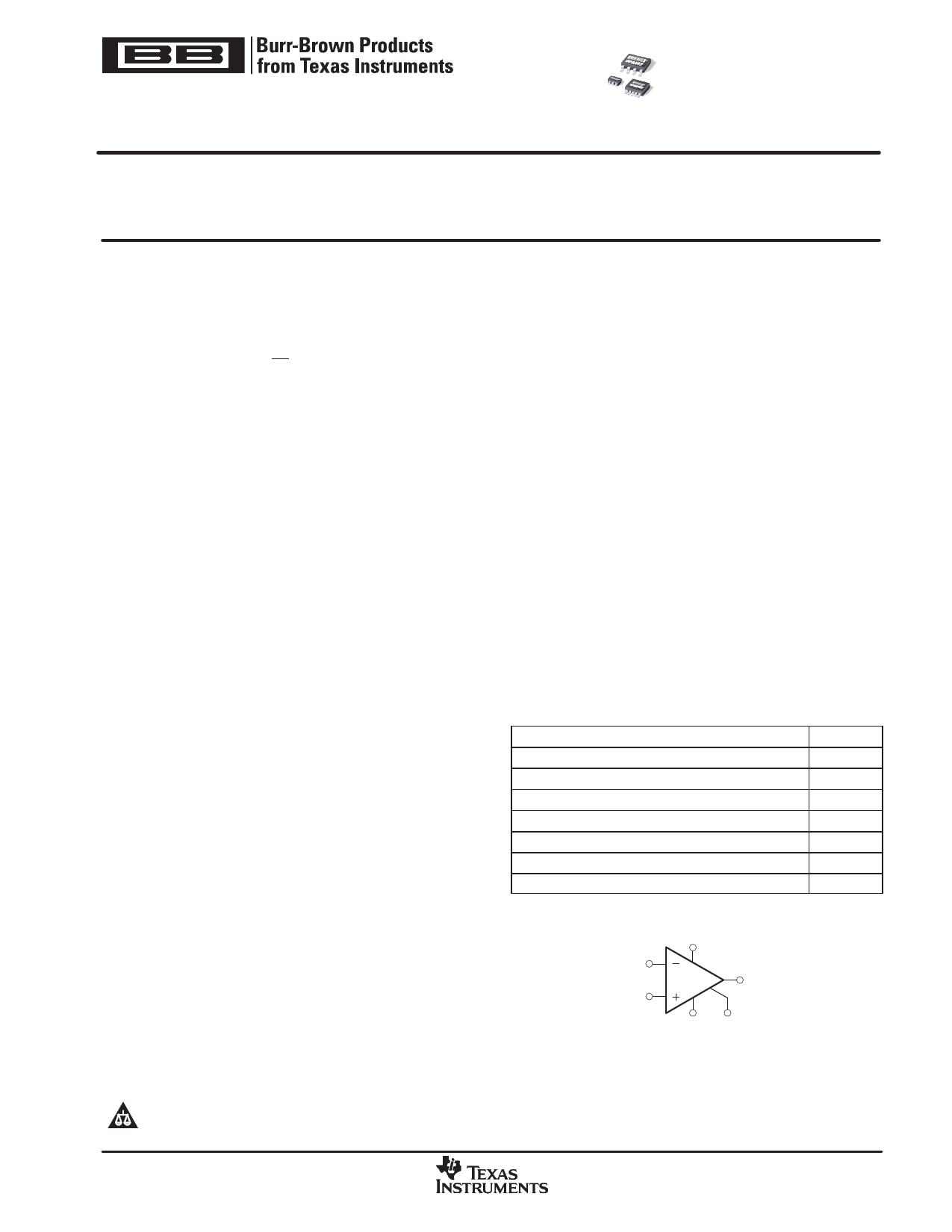
− VIN
+VIN
V+
OPA357
VOUT
V− Enable
Please be aware that an important notice concerning availability, standard warranty, and use in critical applications of Texas Instruments
semiconductor products and disclaimers thereto appears at the end of this data sheet.
All trademarks are the property of their respective owners.
PRODUCTION DATA information is current as of publication date. Products
conform to specifications per the terms of Texas Instruments standard warranty.
Production processing does not necessarily include testing of all parameters.
Copyright 2002-2004, Texas Instruments Incorporated
www.ti.com
1 page 
www.ti.com
OPA357
OPA2357
SBOS235C − MARCH 2002− REVISED MAY 2004
TYPICAL CHARACTERISTICS
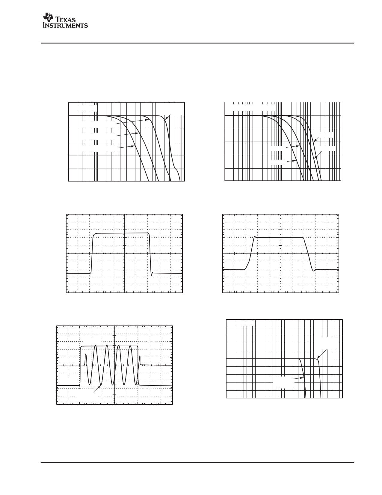
At TA = +25°C, VS = 5V, G = +1, RF = 0Ω, RL = 1kΩ, and connected to VS/2, unless otherwise noted.
NONINVERTING SMALL−SIGNAL
FREQUENCY RESPONSE
3
VO = 0.1VPP
0
G = +1
RF = 25Ω
G = +2, RF = 604Ω
−3
G = +5, RF = 604Ω
−6
G = +10, RF = 604Ω
−9
−12
−15
100k
1M
10M
100M
Frequency (Hz)
1G
NONINVERTING SMALL−SIGNAL STEP RESPONSE
INVERTING SMALL−SIGNAL
FREQUENCY RESPONSE
3
VO = 0.1VPP, RF = 604Ω
0
−3
G = −1
−6
G = −5
G = −2
−9
G = −10
−12
−15
100k
1M
10M
100M
Frequency (Hz)
1G
NONINVERTING LARGE−SIGNAL STEP RESPONSE
Time (20ns/div)
LARGE−SIGNAL DISABLE/ENABLE RESPONSE
Enabled
Disabled
VOUT
fIN = 5MHz
Time (200ns/div)
4.5
3.5
2.5
1.5
0.5
Time (20ns/div)
0.5
VO = 0.1VPP
0.4
0.1dB GAIN FLATNESS
0.3
G = +1
0.2 RF = 25Ω
0.1
0
−0.1
−0.2
−0.3
−0.4
G = +2
RF = 604Ω
−0.5
100k
1M
10M
100M
Frequency (Hz)
1G
5
5 Page 
www.ti.com
APPLICATIONS INFORMATION
The OPA357 is a CMOS, rail-to-rail I/O, high-speed,
voltage-feedback operational amplifier designed for video,
high-speed, and other applications. It is available as a
single or dual op amp.
The amplifier features a 100MHz gain bandwidth, and
150V/µs slew rate, but it is unity-gain stable and can be
operated as a +1V/V voltage follower.
OPERATING VOLTAGE
The OPA357 is specified over a power-supply range of
+2.7V to +5.5V (±1.35V to ±2.75V). However, the supply
voltage may range from +2.5V to +5.5V (±1.25V to
±2.75V). Supply voltages higher than 7.5V (absolute
maximum) can permanently damage the amplifier.
Parameters that vary over supply voltage or temperature
are shown in the Typical Characteristics section of this
data sheet.
ENABLE FUNCTION
The OPA357’s Enable function is implemented using a
Schmitt trigger. The amplifier is enabled by applying a TTL
HIGH voltage level (referenced to V−) to the Enable pin.
Conversely, a TTL LOW voltage level (referenced to V−)
will disable the amplifier, reducing its supply current from
4.9mA to only 3.4µA per amplifier. Independent Enable
pins are available for each channel (dual version),
providing maximum design flexibility. For portable
battery-operated applications, this feature can be used to
greatly reduce the average current and thereby extend
battery life.
OPA357
OPA2357
SBOS235C − MARCH 2002− REVISED MAY 2004
The Enable input can be modeled as a CMOS input gate
with a 100kΩ pull-up resistor to V+. This pin should be
connected to a valid high or low voltage or driven, not left
open circuit.
The enable time is 100ns and the disable time is only 30ns.
This allows the OPA357 to be operated as a gated
amplifier, or to have its output multiplexed onto a common
output bus. When disabled, the output assumes a
high-impedance state.
RAIL-TO-RAIL INPUT
The specified input common-mode voltage range of the
OPA357 extends 100mV beyond the supply rails. This is
achieved with a complementary input stagean
N-channel input differential pair in parallel with a
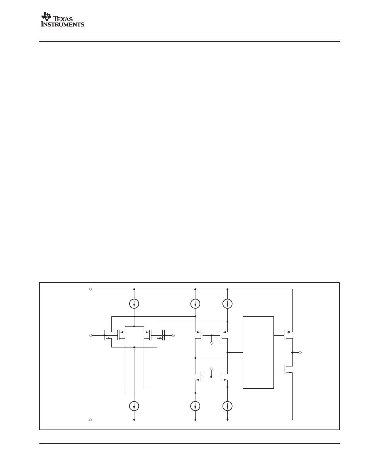
P-channel differential pair, as shown in Figure 1. The
N-channel pair is active for input voltages close to the
positive rail, typically (V+) − 1.2V to 100mV above the
positive supply, while the P-channel pair is on for inputs
from 100mV below the negative supply to approximately
(V+) − 1.2V. There is a small transition region, typically
(V+) − 1.5V to (V+) − 0.9V, in which both pairs are on. This
600mV transition region can vary ±500mV with process
variation. Thus, the transition region (both input stages on)
can range from (V+) − 2.0V to (V+) − 1.5V on the low end,
up to (V+) − 0.9V to (V+) − 0.4V on the high end.
A double-folded cascode adds the signal from the two
input pairs and presents a differential signal to the class AB
output stage.
V+
Reference
Current
VIN+
VIN−
VBIAS1
VBIAS2
Class AB
Control
Circuitry
VO
V−
(Ground)
Figure 1. Simplified Schematic
11
11 Page | ||
| Páginas | Total 23 Páginas | |
| PDF Descargar | [ Datasheet OPA2357.PDF ] | |
Hoja de datos destacado
| Número de pieza | Descripción | Fabricantes |
| OPA2350 | OPAx350 High-Speed Single-Supply Rail-to-Rail Operational Amplifiers MicroAmplifier Series (Rev. D) | Texas Instruments |
| OPA2350 | High-Speed / Single-Supply / Rail-to-Rail OPERATIONAL AMPLIFIERS MicroAmplifier Series | Burr-Brown |
| OPA2353 | High-Speed Single-Supply Rail-to-Rail Op Amps MicroAmplifier | Texas Instruments |
| OPA2353 | High-Speed / Single-Supply / Rail-to-Rail OPERATIONAL AMPLIFIERS MicroAmplifier Series | Burr-Brown |
| Número de pieza | Descripción | Fabricantes |
| SLA6805M | High Voltage 3 phase Motor Driver IC. |
Sanken |
| SDC1742 | 12- and 14-Bit Hybrid Synchro / Resolver-to-Digital Converters. |
Analog Devices |
|
DataSheet.es es una pagina web que funciona como un repositorio de manuales o hoja de datos de muchos de los productos más populares, |
| DataSheet.es | 2020 | Privacy Policy | Contacto | Buscar |
