|
|
|
PDF NTMS7N03R2 Data sheet ( Hoja de datos )
| Número de pieza | NTMS7N03R2 | |
| Descripción | Power MOSFET 7 Amps / 30 Volts | |
| Fabricantes | ON Semiconductor | |
| Logotipo | ||
Hay una vista previa y un enlace de descarga de NTMS7N03R2 (archivo pdf) en la parte inferior de esta página. Total 12 Páginas | ||
|
No Preview Available !
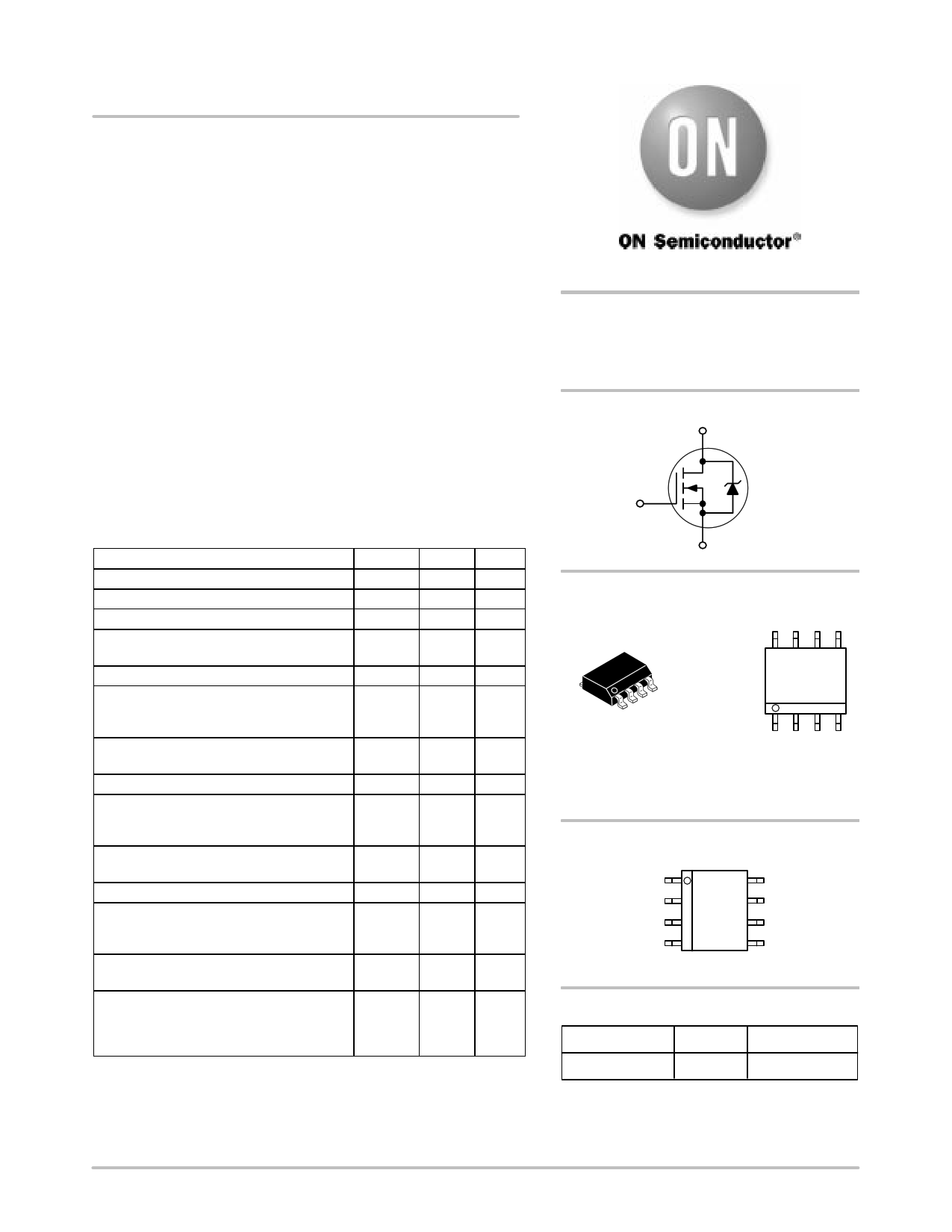
NTMS7N03R2
Power MOSFET
7 Amps, 30 Volts
N-Channel SO-8
Features
• Ultra Low RDS(on)
• Higher Efficiency Extending Battery Life
• Logic Level Gate Drive
• Miniature SO-8 Surface Mount Package
• Avalanche Energy Specified
• IDSS Specified at Elevated Temperature
Typical Applications
• DC-DC Converters
• Power Management
• Motor Controls
• Inductive Loads
• Replaces MMSF7N03HD, MMSF7N03Z, and MMSF5N03HD in
Many Applications
MAXIMUM RATINGS (TC = 25°C unless otherwise noted)
Rating
Symbol Value
Unit
Drain-to-Source Voltage
Drain-to-Gate Voltage (RGS = 1.0 MΩ)
Gate-to-Source Voltage - Continuous
Thermal Resistance - Junction to Ambient
(Note 1)
VDSS
VDGR
VGS
RθJA
30 Vdc
30 Vdc
± 20 Vdc
50 °C/W
Total Power Dissipation @ TA = 25°C
Drain Current - Continuous @ TA = 25°C
Drain Current - Continuous @ TA = 70°C
Drain Current - Pulsed (Note 4)
Thermal Resistance - Junction to Ambient
(Note 2)
PD
ID
ID
IDM
RθJA
2.5 Watts
8.5 Adc
6.8
25 Apk
85 °C/W
Total Power Dissipation @ TA = 25°C
Drain Current - Continuous @ TA = 25°C
Drain Current - Continuous @ TA = 70°C
Drain Current - Pulsed (Note 4)
Thermal Resistance - Junction to Ambient
(Note 3)
PD
ID
ID
IDM
RθJA
1.47 Watts
6.5 Adc
5.2
18 Apk
156 °C/W
Total Power Dissipation @ TA = 25°C
Drain Current - Continuous @ TA = 25°C
Drain Current - Continuous @ TA = 70°C
Drain Current - Pulsed (Note 4)
Operating and Storage Temperature Range
PD
ID
ID
IDM
TJ, Tstg
0.8
4.8
3.8
14
- 55 to
+150
Watts
Adc
Apk
°C
Single Pulse Drain-to-Source Avalanche
Energy - Starting TJ = 25°C
(VDD = 30 Vdc, VGS = 10 Vdc, Peak
IL = 12 Apk, L = 4.0 mH, RG = 25 Ω)
EAS 288 mJ
1. 2″ SQ. FR-4 PCB mounting, (2 oz. Cu 0.06″ thick single sided), 10 Sec. Max.
2. 2″ SQ. FR-4 PCB mounting, (2 oz. Cu 0.06″ thick single sided),
t = steady state.
3. Minimum FR4 or G10 PCB, t = steady state.
4. Pulse test: Pulse Width = 300 µs, Duty Cycle = 2%.
http://onsemi.com
7 AMPERES
30 VOLTS
RDS(on) = 23 mW
N-Channel
D
G
S
MARKING
DIAGRAM
SO-8
8 CASE 751
STYLE 13
1
E7N03
AYWW
E7N03
A
Y
WW
= Device Code
= Assembly Location
= Year
= Work Week
PIN ASSIGNMENT
N-C
Source
Source
Gate
18
27
36
45
Top View
Drain
Drain
Drain
Drain
ORDERING INFORMATION
Device
Package
Shipping
NTMS7N03R2
SO-8 2500/Tape & Reel
© Semiconductor Components Industries, LLC, 2002
November, 2002 - Rev. 3
1
Publication Order Number:
NTMS7N03R2/D
1 page 
NTMS7N03R2
POWER MOSFET SWITCHING
Switching behavior is most easily modeled and predicted
by recognizing that the power MOSFET is charge
controlled. The lengths of various switching intervals (∆t)
are determined by how fast the FET input capacitance can
be charged by current from the generator.
The published capacitance data is difficult to use for
calculating rise and fall because drain-gate capacitance
varies greatly with applied voltage. Accordingly, gate
charge data is used. In most cases, a satisfactory estimate of
average input current (IG(AV)) can be made from a
rudimentary analysis of the drive circuit so that
t = Q/IG(AV)
During the rise and fall time interval when switching a
resistive load, VGS remains virtually constant at a level
known as the plateau voltage, VSGP. Therefore, rise and fall
times may be approximated by the following:
tr = Q2 x RG/(VGG - VGSP)
tf = Q2 x RG/VGSP
where
VGG = the gate drive voltage, which varies from zero to VGG
RG = the gate drive resistance
and Q2 and VGSP are read from the gate charge curve.
During the turn-on and turn-off delay times, gate current is
not constant. The simplest calculation uses appropriate
values from the capacitance curves in a standard equation for
voltage change in an RC network. The equations are:
td(on) = RG Ciss In [VGG/(VGG - VGSP)]
td(off) = RG Ciss In (VGG/VGSP)
The capacitance (Ciss) is read from the capacitance curve at
a voltage corresponding to the off-state condition when
calculating td(on) and is read at a voltage corresponding to the
on-state when calculating td(off).
At high switching speeds, parasitic circuit elements
complicate the analysis. The inductance of the MOSFET
source lead, inside the package and in the circuit wiring
which is common to both the drain and gate current paths,
produces a voltage at the source which reduces the gate drive
current. The voltage is determined by Ldi/dt, but since di/dt
is a function of drain current, the mathematical solution is
complex. The MOSFET output capacitance also
complicates the mathematics. And finally, MOSFETs have
finite internal gate resistance which effectively adds to the
resistance of the driving source, but the internal resistance
is difficult to measure and, consequently, is not specified.
The resistive switching time variation versus gate
resistance (Figure 9) shows how typical switching
performance is affected by the parasitic circuit elements. If
the parasitics were not present, the slope of the curves would
maintain a value of unity regardless of the switching speed.
The circuit used to obtain the data is constructed to minimize
common inductance in the drain and gate circuit loops and
is believed readily achievable with board mounted
components. Most power electronic loads are inductive; the
data in the figure is taken with a resistive load, which
approximates an optimally snubbed inductive load. Power
MOSFETs may be safely operated into an inductive load;
however, snubbing reduces switching losses.
2800 VDS = 0 V VGS = 0 V
2400
2000
Ciss
TJ = 25°C
1600 Crss
1200
Ciss
800
400
0
10
Crss
505
VGS
VDS
Coss
10 15 20
GATE-T O-SOURCE OR DRAIN-TO-SOURCE VOLTAGE (VOLTS)
Figure 7. Capacitance Variation
http://onsemi.com
5
5 Page 
NTMS7N03R2
PACKAGE DIMENSIONS
-X-
A
SO-8
CASE 751-07
ISSUE AA
B
-Y-
-Z-
H
85
S 0.25 (0.010) M Y M
1
4
K
G
D
C
SEATING
PLANE
N X 45 _
0.10 (0.004)
M
0.25 (0.010) M Z Y S X S
J
NOTES:
1. DIMENSIONING AND TOLERANCING PER ANSI
Y14.5M, 1982.
2. CONTROLLING DIMENSION: MILLIMETER.
3. DIMENSION A AND B DO NOT INCLUDE MOLD
PROTRUSION.
4. MAXIMUM MOLD PROTRUSION 0.15 (0.006) PER
SIDE.
5. DIMENSION D DOES NOT INCLUDE DAMBAR
PROTRUSION. ALLOWABLE DAMBAR
PROTRUSION SHALL BE 0.127 (0.005) TOTAL IN
EXCESS OF THE D DIMENSION AT MAXIMUM
MATERIAL CONDITION.
6. 751−01 THRU 751−06 ARE OBSOLETE. NEW
STANDARD IS 751−07.
MILLIMETERS
INCHES
DIM MIN MAX MIN MAX
A 4.80 5.00 0.189 0.197
B 3.80 4.00 0.150 0.157
C 1.35 1.75 0.053 0.069
D 0.33 0.51 0.013 0.020
G 1.27 BSC
0.050 BSC
H 0.10 0.25 0.004 0.010
J 0.19 0.25 0.007 0.010
K 0.40 1.27 0.016 0.050
M 0_ 8_ 0_ 8_
N 0.25 0.50 0.010 0.020
S 5.80 6.20 0.228 0.244
STYLE 13:
PIN 1. N.C.
2. SOURCE
3. SOURCE
4. GATE
5. DRAIN
6. DRAIN
7. DRAIN
8. DRAIN
http://onsemi.com
11
11 Page | ||
| Páginas | Total 12 Páginas | |
| PDF Descargar | [ Datasheet NTMS7N03R2.PDF ] | |
Hoja de datos destacado
| Número de pieza | Descripción | Fabricantes |
| NTMS7N03R2 | Power MOSFET 7 Amps / 30 Volts | ON Semiconductor |
| Número de pieza | Descripción | Fabricantes |
| SLA6805M | High Voltage 3 phase Motor Driver IC. |
Sanken |
| SDC1742 | 12- and 14-Bit Hybrid Synchro / Resolver-to-Digital Converters. |
Analog Devices |
|
DataSheet.es es una pagina web que funciona como un repositorio de manuales o hoja de datos de muchos de los productos más populares, |
| DataSheet.es | 2020 | Privacy Policy | Contacto | Buscar |