|
|
PDF NE5210D Data sheet ( Hoja de datos )
| Número de pieza | NE5210D | |
| Descripción | Transimpedance amplifier 280MHz | |
| Fabricantes | Philips | |
| Logotipo |  |
|
Hay una vista previa y un enlace de descarga de NE5210D (archivo pdf) en la parte inferior de esta página. Total 14 Páginas | ||
|
No Preview Available !
Philips Semiconductors
Transimpedance amplifier (280MHz)
Product specification
NE5210
DESCRIPTION
The NE5210 is a 7kΩ transimpedance wide band, low noise
amplifier with differential outputs, particularly suitable for signal
recovery in fiber-optic receivers. The part is ideally suited for many
other RF applications as a general purpose gain block.
FEATURES
• Low noise: 3.5pA/√Hz
• Single 5V supply
• Large bandwidth: 280MHz
• Differential outputs
• Low input/output impedances
• High power supply rejection ratio
• High overload threshold current
• Wide dynamic range
• 7kΩ differential transresistance
APPLICATIONS
• Fiber-optic receivers, analog and digital
• Current-to-voltage converters
PIN CONFIGURATION
D Package
GND2 1
GND2 2
NC 3
IIN 4
NC 5
VCC1 6
VCC2 7
14 OUT (–)
13 GND2
12 OUT (+)
11 GND1
10 GND1
9 GND1
8 GND1
TOP VIEW
• Wideband gain block
• Medical and scientific instrumentation
• Sensor preamplifiers
• Single-ended to differential conversion
• Low noise RF amplifiers
• RF signal processing
SD00318
ORDERING INFORMATION
DESCRIPTION
14-Pin Plastic Small Outline (SO) Package
TEMPERATURE RANGE
0 to +70°C
ORDER CODE
NE5210D
DWG #
SOT108-1
ABSOLUTE MAXIMUM RATINGS
SYMBOL
PARAMETER
RATING
VCC
TA
TJ
TSTG
PDMAX
IINMAX
Power supply
Operating ambient temperature range
Operating junction temperature range
Storage temperature range
Power dissipation, TA=25°C (still air)1
Maximum input current2
6
0 to +70
-55 to +150
-65 to +150
1.0
5
NOTES:
1. Maximum dissipation is determined by the operating ambient temperature and the thermal resistance: θJA=125°C/W.
2. The use of a pull-up resistor to VCC for the PIN diode, is recommended.
RECOMMENDED OPERATING CONDITIONS
SYMBOL
PARAMETER
VCC Supply voltage
TA Ambient temperature range
TJ Junction temperature range
RATING
4.5 to 5.5
0 to +70
0 to +90
UNIT
V
°C
°C
°C
W
mA
UNIT
V
°C
°C
1995 Apr 26
1 853-1654 15170
1 page 
Philips Semiconductors
Transimpedance amplifier (280MHz)
Product specification
NE5210
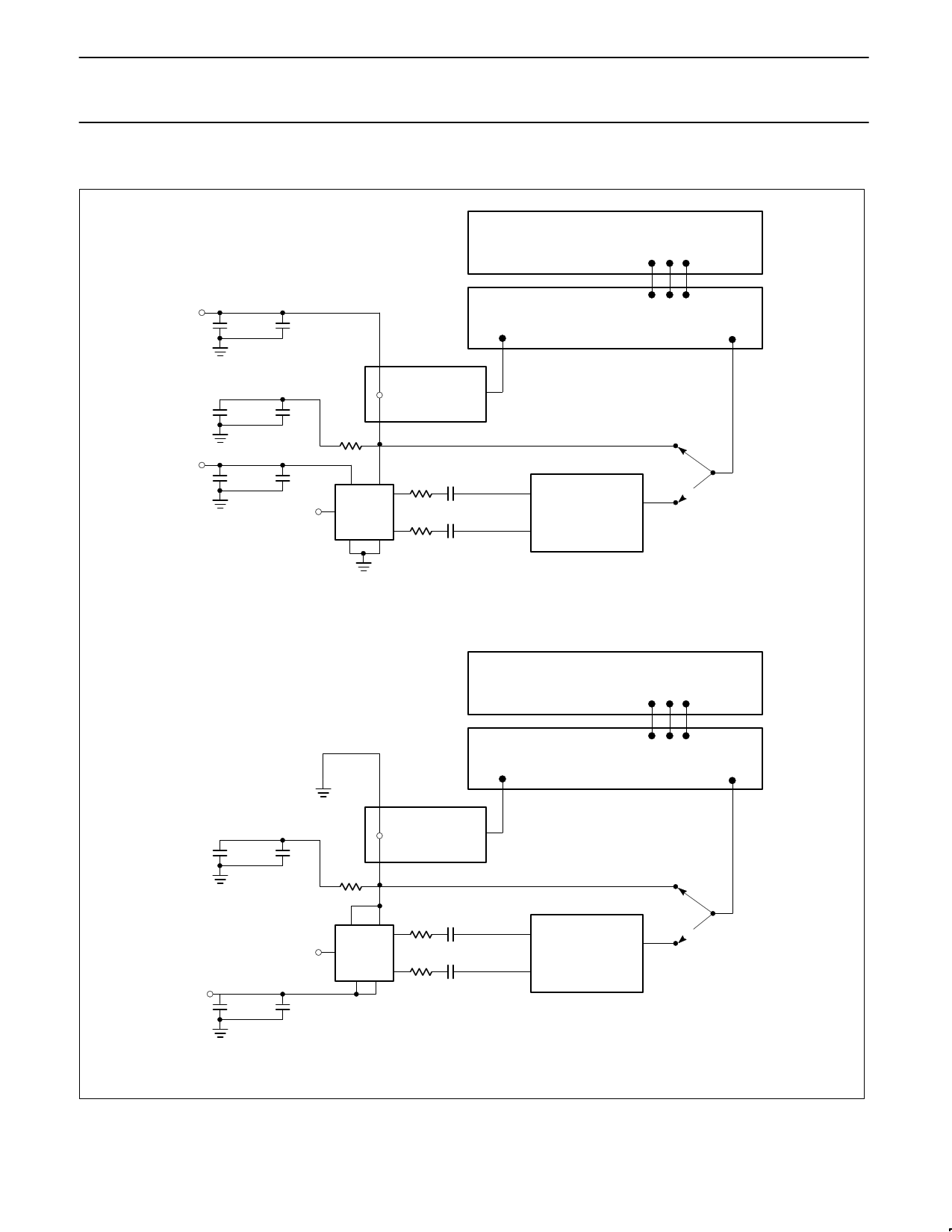
TEST CIRCUITS (Continued)
NETWORK ANALYZER
5V
10µF
0.1µF
PORT 1
S-PARAMETER TEST SET
PORT 2
10µF
0.1µF
CURRENT PROBE
1mV/mA
16
CAL
5V
10µF
VCC1
VCC2 33 0.1µF
0.1µF
IN
OUT
OUT
33
100
BAL.
TRANSFORMER
NH0300HB
50 TEST
UNBAL.
GND1
GND2
0.1µF
Test Circuit 5
NETWORK ANALYZER
GND
PORT 1
S-PARAMETER TEST SET
PORT 2
5.2V
10µF
0.1µF
CURRENT PROBE
1mV/mA
16
10µF
GND1
IN
VCC1
GND2 33
OUT
OUT
33
VCC2
0.1µF
0.1µF
0.1µF
CAL
100
BAL.
TRANSFORMER
NH0300HB
50 TEST
UNBAL.
Test Circuit 6
SD00321
1995 Apr 26
5
5 Page 
Philips Semiconductors
Transimpedance amplifier (280MHz)
Product specification
NE5210
THEORY OF OPERATION
Transimpedance amplifiers have been widely used as the
preamplifier in fiber-optic receivers. The NE5210 is a wide
bandwidth (typically 280MHz) transimpedance amplifier designed
primarily for input currents requiring a large dynamic range, such as
those produced by a laser diode. The maximum input current before
output stage clipping occurs at typically 240µA. The NE5210 is a
bipolar transimpedance amplifier which is current driven at the input
and generates a differential voltage signal at the outputs. The
forward transfer function is therefore a ratio of the differential output
voltage to a given input current with the dimensions of ohms. The
main feature of this amplifier is a wideband, low-noise input stage
which is desensitized to photodiode capacitance variations. When
connected to a photodiode of a few picoFarads, the frequency
response will not be degraded significantly. Except for the input
stage, the entire signal path is differential to provide improved
power-supply rejection and ease of interface to ECL type circuitry. A
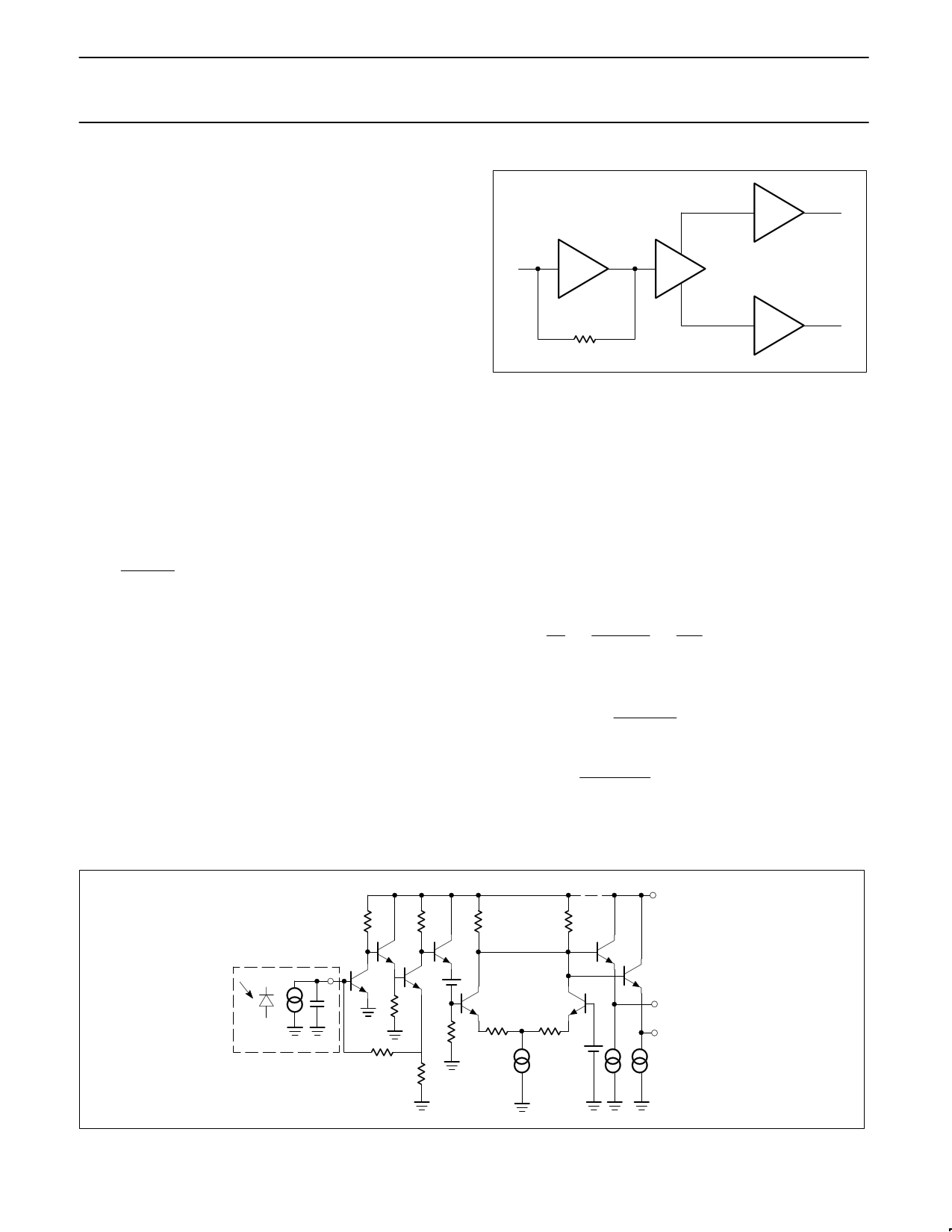
block diagram of the circuit is shown in Figure 1. The input stage
(A1) employs shunt-series feedback to stabilize the current gain of
the amplifier. The transresistance of the amplifier from the current
source to the emitter of Q3 is approximately the value of the
feedback resistor, RF=3.6kΩ. The gain from the second stage (A2)
and emitter followers (A3 and A4) is about two. Therefore, the
differential transresistance of the entire amplifier, RT is
RT
+
VOUT(diff)
IIN
+ 2RF
+ 2(3.6K)
+ 7.2kW
The single-ended transresistance of the amplifier is typically 3.6kΩ.
The simplified schematic in Figure 2 shows how an input current is
converted to a differential output voltage. The amplifier has a single
input for current which is referenced to Ground 1. An input current
from a laser diode, for example, will be converted into a voltage by
the feedback resistor RF. The transistor Q1 provides most of the
open loop gain of the circuit, AVOL≈70. The emitter follower Q2
minimizes loading on Q1. The transistor Q4, resistor R7, and VB1
provide level shifting and interface with the Q15 – Q16 differential
pair of the second stage which is biased with an internal reference,
VB2. The differential outputs are derived from emitter followers Q11 –
Q12 which are biased by constant current sources. The collectors of
Q11 – Q12 are bonded to an external pin, VCC2, in order to reduce
the feedback to the input stage. The output impedance is about 17Ω
single-ended. For ease of performance evaluation, a 33Ω resistor is
used in series with each output to match to a 50Ω test system.
OUTPUT +
A3
INPUT
A1
A2
RF A4
Figure 1. NE5210 – Block Diagram
OUTPUT –
SD00327
BANDWIDTH CALCULATIONS
The input stage, shown in Figure 3, employs shunt-series feedback
to stabilize the current gain of the amplifier. A simplified analysis can
determine the performance of the amplifier. The equivalent input
capacitance, CIN, in
parallel with the source, IS, is approximately 7.5pF, assuming that
CS=0 where CS is the external source capacitance.
Since the input is driven by a current source the input must have a
low input resistance. The input resistance, RIN, is the ratio of the
incremental input voltage, VIN, to the corresponding input current, IIN
and can be calculated as:
RIN
+
VIN
IIN
+
1
RF
) AVOL
+
3.6K
71
+ 51W
More exact calculations would yield a higher value of 60Ω.
Thus CIN and RIN will form the dominant pole of the entire amplifier;
f*3dB + 2p
1
RIN CIN
Assuming typical values for RF = 3.6kΩ, RIN = 60Ω, CIN = 7.5pF
f*3dB + 2p
1
7.5pF 60
+ 354MHz
VCC1
R1 R3
R12
VCC2
R13
INPUT
Q2
Q1 Q3
Q4
+
PHOTODIODE
GND1
R2
Q15
R14
R7
R5
R4
Q16
R15
VB2
GND2
Q11
Q12
OUT–
+ OUT+
Figure 2. Transimpedance Amplifier
SD00328
1995 Apr 26
11
11 Page | ||
| Páginas | Total 14 Páginas | |
| PDF Descargar | [ Datasheet NE5210D.PDF ] | |
Hoja de datos destacado
| Número de pieza | Descripción | Fabricantes |
| NE5210 | Transimpedance amplifier 280MHz | Philips |
| NE5210D | Transimpedance amplifier 280MHz | Philips |
| Número de pieza | Descripción | Fabricantes |
| SLA6805M | High Voltage 3 phase Motor Driver IC. |
Sanken |
| SDC1742 | 12- and 14-Bit Hybrid Synchro / Resolver-to-Digital Converters. |
Analog Devices |
|
DataSheet.es es una pagina web que funciona como un repositorio de manuales o hoja de datos de muchos de los productos más populares, |
| DataSheet.es | 2020 | Privacy Policy | Contacto | Buscar |
