|
|
PDF NE1619DS Data sheet ( Hoja de datos )
| Número de pieza | NE1619DS | |
| Descripción | Temperature and voltage monitor | |
| Fabricantes | Philips | |
| Logotipo |  |
|
Hay una vista previa y un enlace de descarga de NE1619DS (archivo pdf) en la parte inferior de esta página. Total 19 Páginas | ||
|
No Preview Available !
INTEGRATED CIRCUITS
NE1619
HECETA4
Temperature and voltage monitor
Product data sheet
Supersedes data of 2004 May 10
2004 Oct 05
Philips
Semiconductors
1 page 
Philips Semiconductors
HECETA4 Temperature and voltage monitor
Product data sheet
NE1619
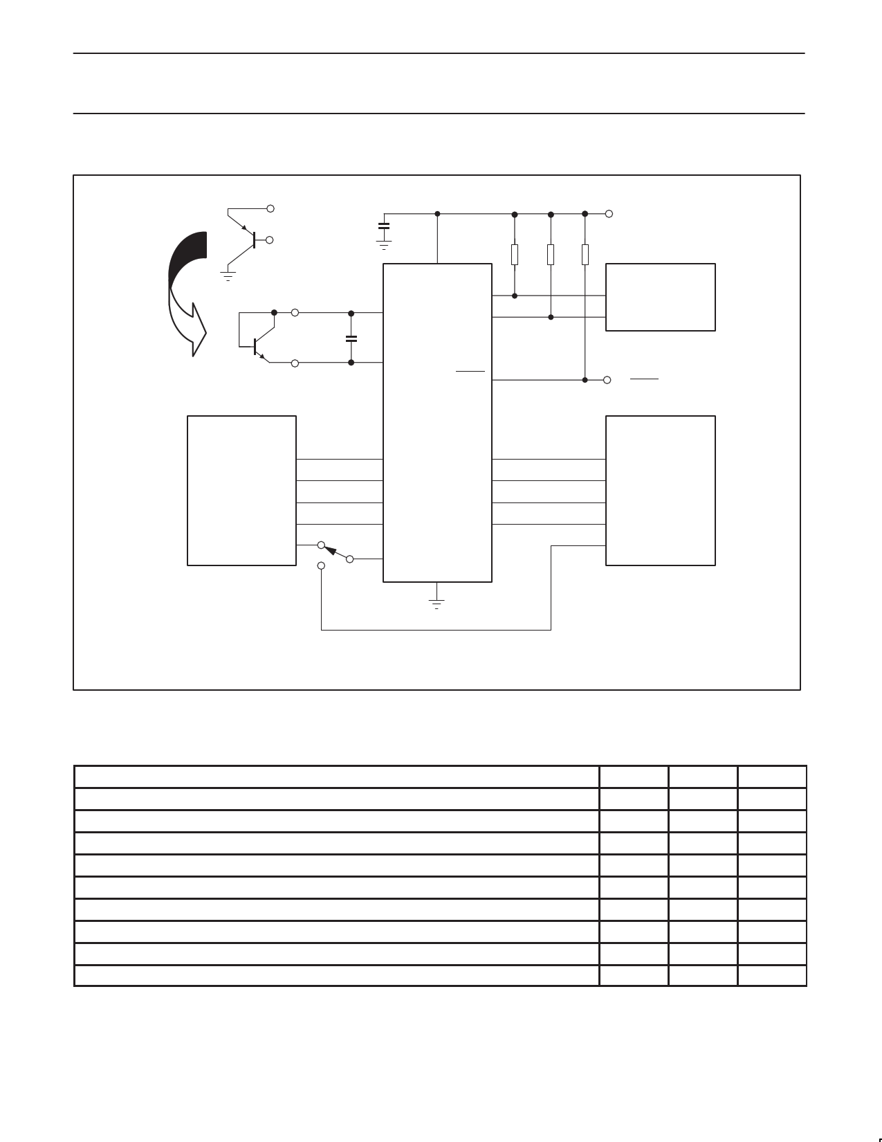
TYPICAL APPLICATION CIRCUIT
Remote Sensor
0.1 µF
Ground
µP On-Board PNP Transistor
See
Note 1
or Discrete NPN Transistor
10
D+
4
VDD/3.3VSB
10 kΩ
2
SCL
1
SDA
10 kΩ
9
D–
A0/RESET/ 16
NTEST_OUT
System Power
Supplies
VCCP
2.5 V
3.3 V
5.0 V
12.0 V
NE1619
15
VCCPVIN
14
2.5VIN
13 3.3VIN
12
5VIN
VID0
VID1
VID2
VID3
5
6
7
8
11 12VIN/VID4
GND
3
Ground
NOTE:
1. Should be placed close to D+ and D– pins.
May be required in noisy environment, about 1 nF.
Figure 3. Typical application circuit
ABSOLUTE MAXIMUM RATINGS
PARAMETER
VDD to GND
12VIN to GND
5VIN, 3.3VIN, 2.5VIN, VCCP to GND
Other pins to GND
Input current at any pin
Package input current
Operating temperature range
Maximum junction temperature
Storage temperature range
VDD
100 kΩ
SMBus
CLOCK
DATA
Selectable
A0/RESET/NTEST_OUT
Processor Voltage
ID Code
VID0
VID1
VID2
VID3
VID4
SL01230
MIN.
–0.3
–0.3
–0.3
–0.3
–5
–20
0
–
–65
MAX.
6
18
6
VDD+0.3
5
20
+125
+150
+150
UNIT
V
V
V
V
mA
mA
°C
°C
°C
2004 Oct 05
5
5 Page 
Philips Semiconductors
HECETA4 Temperature and voltage monitor
Product data sheet
NE1619
Table 2. Configuration Register (CR, 40h, default = 0000 1000)
BIT NAME
R/W
DESCRIPTION
0 START
R/W Logic 1 enables startup of monitor device, logic 0 places the device in standby mode.
Power–up default = 0.
At startup, limit checking functions and scanning begins. Note, all High and Low limits
should be set into the ASIC prior turning on this bit.
1 Reserved
Read
Power-up default = 0.
2 Reserved
Read
Power-up default = 0.
3 Reserved
Read
Power-up default = 1.
4 RESET
5 12VIN/VID4
SELECT
6 Reserved
R/W
R/W
Read
Setting this bit generates a minimum 20ms low pulse on the Reset pin, if the reset
function is enabled. Power-up default = 0.
Selects whether pin 11 acts as a 12 volt analog input monitoring pin, or as a VID[4] input.
This pin defaults to the 12 volt analog input. Power–up default = 0.
Power–up default = 0.
7 Initialization
R/W Logic 1 restores power–up default values to the configuration register and the status
registers. This bit automatically clears itself. Power–up default = 0.
Table 3. Status Register 1 (SR1, 41h, default = 0000 0000)
BIT NAME
R/W
DESCRIPTION
0 +2.5V_ERROR
Read
A one indicates 2.5VIN High or Low limit has been exceeded.
1 VCCP_ERROR
2 +3.3V_ERROR
3 +5V_ERROR
4 Internal Temp Error
5 External Temp Error
6 Reserved
7 Reserved
Read
Read
Read
Read
Read
Read
Read
A one indicates VCCPVIN High or Low limit has been exceeded.
A one indicates 3.3VIN High or Low limit has been exceeded.
A one indicates 5VIN High or Low limit has been exceeded.
A one indicates internal or local temp High or Low limit has been exceeded.
A one indicates external or remote temp High or Low limit has been exceeded.
Table 4. Status Register 2 (SR2, 42h, default = 0000 0000)
BIT NAME
R/W
DESCRIPTION
0 +12V_ERROR
1 VDD_ERROR
2 Reserved
Read
Read
Read
A one indicates 12VIN High or Low limit has been exceeded.
A one indicates VDD High or Low limit has been exceeded.
Undefined.
3 Reserved
Read
Undefined.
4 Reserved
Read
Undefined.
5 Reserved
Read
Undefined.
6 Remote Diode Fault
Read
A one indicates either a short or open circuited fault on the remote thermal diode inputs.
7 Reserved
Read
Undefined.
Table 5. VID (VID, 47h, default = 0000 VID[3:0] )
BIT NAME
R/W
DESCRIPTION
0–3 VID[0:3]
Read
The VID[0:3] inputs from Pentium/PRO power supplies ID to indicate the operating
voltage (e.g. 1.5V to 2.9V). Power-up default = VID[0:3].
4–6 Reserved
Read
Undefined.
7 RESET ENABLE
Read
When set to 1, enables the RESET pin output function.
This bit defaults to 0 at Power–up and enables addressing function.
Table 6. VID4 (VID4, 49h, default = 1000 000VID[4] )
BIT NAME
R/W
DESCRIPTION
0 VID4
Read
VID4 input, if selected, from Pentium/PRO power supplied ID.
Power-up default = 0 and pin 11 is not selected for VID4.
1–7 Reserved
Read
Power-up default = 1000 000
2004 Oct 05
11
11 Page | ||
| Páginas | Total 19 Páginas | |
| PDF Descargar | [ Datasheet NE1619DS.PDF ] | |
Hoja de datos destacado
| Número de pieza | Descripción | Fabricantes |
| NE1619DS | Temperature and voltage monitor | Philips |
| Número de pieza | Descripción | Fabricantes |
| SLA6805M | High Voltage 3 phase Motor Driver IC. |
Sanken |
| SDC1742 | 12- and 14-Bit Hybrid Synchro / Resolver-to-Digital Converters. |
Analog Devices |
|
DataSheet.es es una pagina web que funciona como un repositorio de manuales o hoja de datos de muchos de los productos más populares, |
| DataSheet.es | 2020 | Privacy Policy | Contacto | Buscar |
