|
|
|
PDF NDB710BE Data sheet ( Hoja de datos )
| Número de pieza | NDB710BE | |
| Descripción | N-Channel Enhancement Mode Field Effect Transistor | |
| Fabricantes | Fairchild | |
| Logotipo | ||
Hay una vista previa y un enlace de descarga de NDB710BE (archivo pdf) en la parte inferior de esta página. Total 6 Páginas | ||
|
No Preview Available !
May 1994
NDP710A / NDP710AE / NDP710B / NDP710BE
NDB710A / NDB710AE / NDB710B / NDB710BE
N-Channel Enhancement Mode Field Effect Transistor
General Description
Features
These N-channel enhancement mode power field
effect transistors are produced using Fairchild's
proprietary, high cell density, DMOS technology. This
very high density process has been especially
tailored to minimize on-state resistance, provide
superior switching performance, and withstand high
energy pulses in the avalanche and commutation
modes. These devices are particularly suited for low
voltage applications such as automotive, DC/DC
converters, PWM motor controls, and other battery
powered circuits where fast switching, low in-line
power loss, and resistance to transients are needed.
42 and 40A, 100V. RDS(ON) = 0.038 and 0.042Ω.
Critical DC electrical parameters specified at
elevated temperature.
Rugged internal source-drain diode can eliminate
the need for an external Zener diode transient
suppressor.
175°C maximum junction temperature rating.
High density cell design (3 million/in²) for extremely
low RDS(ON).
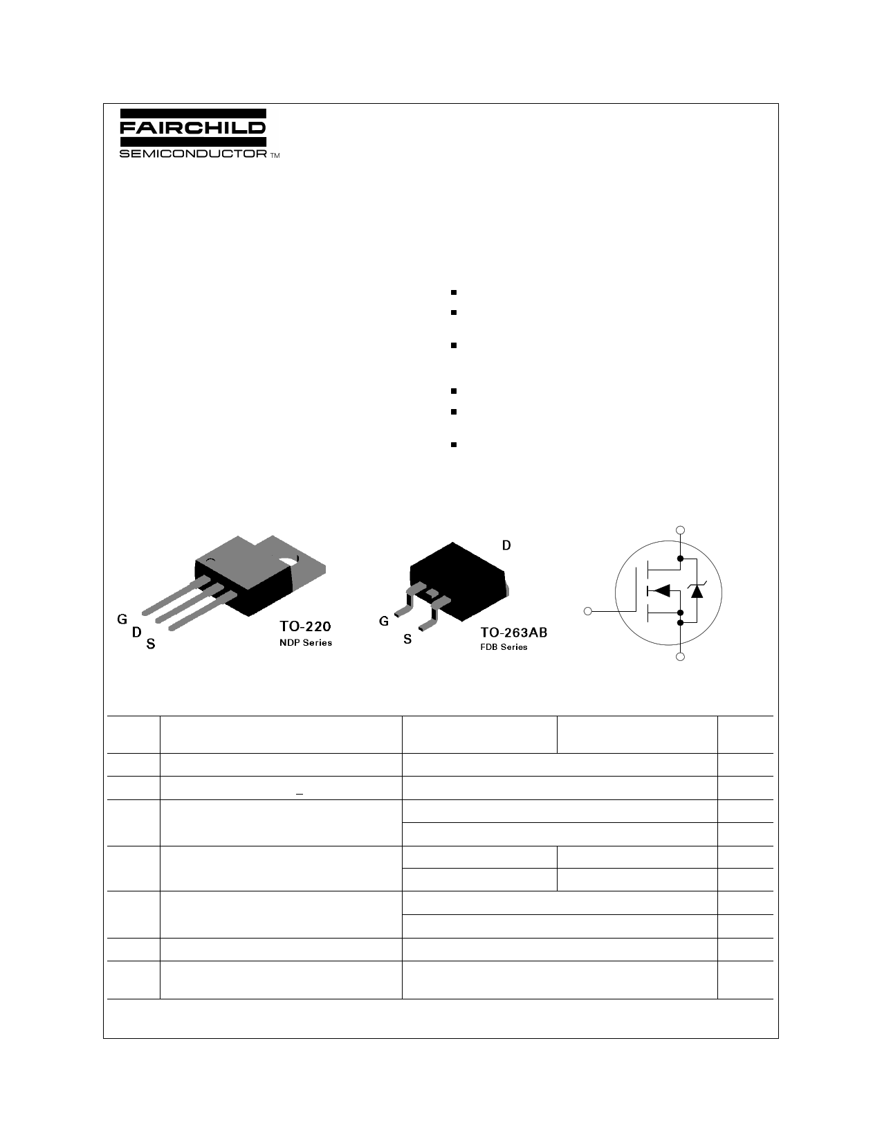
TO-220 and TO-263 (D2PAK) package for both
through hole and surface mount applications.
_____________________________________________________________________
D
G
S
Absolute Maximum Ratings
Symbol Parameter
TC = 25°C unless otherwise noted
NDP710A NDP710AE
NDB710A NDB710AE
NDP710B NDP710BE
NDB710B NDB710BE
VDSS Drain-Source Voltage
VDGR
Drain-Gate Voltage (RGS < 1 MΩ)
VGSS Gate-Source Voltage - Continuous
- Nonrepetitive (tP < 50 µs)
ID Drain Current - Continuous
- Pulsed
100
100
±20
±40
42 40
168 160
PD Total Power Dissipation @ TC = 25°C
Derate above 25°C
150
1
TJ,TSTG
TL
Operating and Storage Temperature Range
Maximum lead temperature for soldering
purposes, 1/8" from case for 5 seconds
-65 to 175
275
Units
V
V
V
V
A
A
W
W/°C
°C
°C
© 1997 Fairchild Semiconductor Corporation
NDP710.SAM
1 page 
Typical Electrical Characteristics (continued)
1.15
I = 250µA
D
1.1
1.05
1
0.95
0.9
-50
-25
0 25 50 75 100 125 150 175
T J , JUNCTION TEMPERATURE (°C)
Figure 7. Breakdown Voltage
Variation with Temperature.
6000
3000
2000
C iss
1000
C oss
300
200
100
0.1
f = 1 MHz
V GS = 0V
C rss
0.2
0.5 1
2
5 10 20
VDS , DRAIN TO SOURCE VOLTAGE (V)
50
Figure 9. Capacitance Characteristics.
30
VGS = 0V
10
TJ = 125°C
25°C
-55°C
1
0.1
0.01
0.2
0.4 0.6 0.8 1 1.2
VSD , BODY DIODE FORWARD VOLTAGE (V)
1.4
Figure 8. Body Diode Forward Voltage
Variation with Current and
Temperature.
20
ID = 42A
15
V DS= 20V
50
80
10
5
0
0 40 80 120 160
Q g , GATE CHARGE (nC)
Figure 10. Gate Charge Characteristics.
VIN
VGS
RGEN
G
VDD
RL
D
V OUT
DUT
S
t d(on)
t on
tr
90%
t d(off)
toff
tf
90%
Output, Vout
Input, Vin
10%
10%
50%
10%
90% Inverted
50%
Pulse Width
Figure 36. Switching Test Circuit.
Figure 12. Switching Waveforms.
NDP710.SAM
5 Page | ||
| Páginas | Total 6 Páginas | |
| PDF Descargar | [ Datasheet NDB710BE.PDF ] | |
Hoja de datos destacado
| Número de pieza | Descripción | Fabricantes |
| NDB710B | N-Channel Enhancement Mode Field Effect Transistor | Fairchild |
| NDB710BE | N-Channel Enhancement Mode Field Effect Transistor | Fairchild |
| Número de pieza | Descripción | Fabricantes |
| SLA6805M | High Voltage 3 phase Motor Driver IC. |
Sanken |
| SDC1742 | 12- and 14-Bit Hybrid Synchro / Resolver-to-Digital Converters. |
Analog Devices |
|
DataSheet.es es una pagina web que funciona como un repositorio de manuales o hoja de datos de muchos de los productos más populares, |
| DataSheet.es | 2020 | Privacy Policy | Contacto | Buscar |