|
|
|
PDF NCV1117 Data sheet ( Hoja de datos )
| Número de pieza | NCV1117 | |
| Descripción | 1.0 A Low-Dropout Positive Fixed and Adjustable Voltage Regulators | |
| Fabricantes | ON | |
| Logotipo | ||
Hay una vista previa y un enlace de descarga de NCV1117 (archivo pdf) en la parte inferior de esta página. Total 17 Páginas | ||
|
No Preview Available !
NCP1117, NCV1117
1.0 A Low-Dropout Positive
Fixed and Adjustable
Voltage Regulators
The NCP1117 series are low dropout positive voltage regulators that
are capable of providing an output current that is in excess of 1.0 A
with a maximum dropout voltage of 1.2 V at 800 mA over
temperature. This series contains nine fixed output voltages of 1.5 V,
1.8 V, 1.9 V, 2.0 V, 2.5 V, 2.85 V, 3.3 V, 5.0 V, and 12 V that have no
minimum load requirement to maintain regulation. Also included is an
adjustable output version that can be programmed from 1.25 V to
18.8 V with two external resistors. On chip trimming adjusts the
reference/output voltage to within ±1.0% accuracy. Internal protection
features consist of output current limiting, safe operating area
compensation, and thermal shutdown. The NCP1117 series can
operate with up to 20 V input. Devices are available in SOT−223 and
DPAK packages.
Features
• Output Current in Excess of 1.0 A
• 1.2 V Maximum Dropout Voltage at 800 mA Over Temperature
• Fixed Output Voltages of 1.5 V, 1.8 V, 1.9 V, 2.0 V, 2.5 V, 2.85 V,
3.3 V, 5.0 V, and 12 V
• Adjustable Output Voltage Option
• No Minimum Load Requirement for Fixed Voltage Output Devices
• Reference/Output Voltage Trimmed to ±1.0%
• Current Limit, Safe Operating and Thermal Shutdown Protection
• Operation to 20 V Input
• NCV Prefix for Automotive and Other Applications Requiring
Unique Site and Control Change Requirements; AEC−Q100
Qualified and PPAP Capable
• These are Pb-Free Devices
Applications
• Consumer and Industrial Equipment Point of Regulation
• Active SCSI Termination for 2.85 V Version
• Switching Power Supply Post Regulation
• Hard Drive Controllers
• Battery Chargers
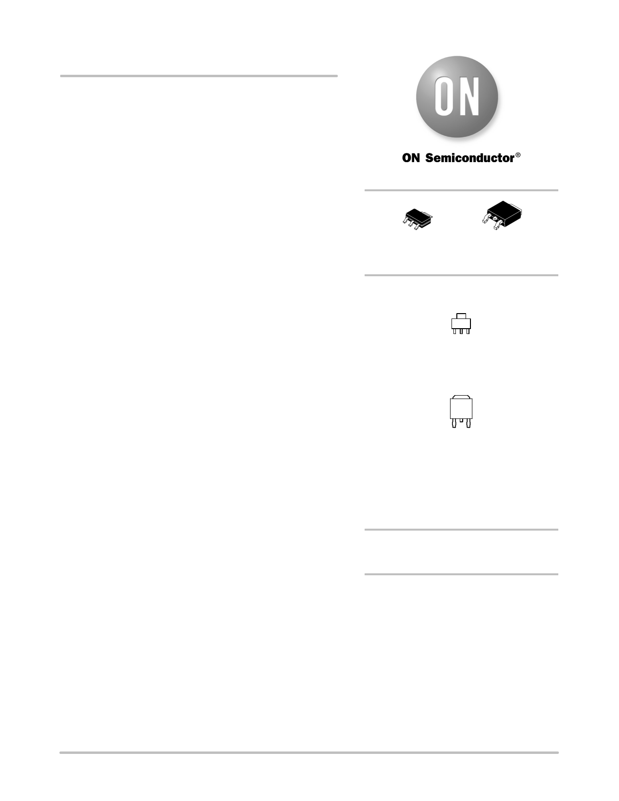
http://onsemi.com
SOT−223
ST SUFFIX
CASE 318H
DPAK
DT SUFFIX
CASE 369C
PIN CONFIGURATION
Tab
123
SOT−223
(Top View)
Tab
123
DPAK
(Top View)
Pin: 1. Adjust/Ground
2. Output
3. Input
Heatsink tab is connected to Pin 2.
ORDERING INFORMATION
See detailed ordering and shipping information in the package
dimensions section on page 12 of this data sheet.
DEVICE MARKING INFORMATION
See general marking information in the device marking
section on page 14 of this data sheet.
© Semiconductor Components Industries, LLC, 2014
September, 2014 − Rev. 27
1
Publication Order Number:
NCP1117/D
1 page 
NCP1117, NCV1117
2.0
1.5
Vin = Vout + 3.0 V
Iout = 10 mA
1.0
Adj, 1.5 V,
1.8 V, 2.0 V,
2.5 V
0.5
0
−0.5
−1.0
2.85 V, 3.3 V,
5.0 V, 12.0 V
−1.5
−2.0
−50
−25 0 25 50 75 100 125 150
TA, AMBIENT TEMPERATURE (°C)
Figure 4. Output Voltage Change
vs. Temperature
1.4
1.2
TJ = −40°C
1.0
TJ = 25°C
0.8
TJ = 125°C
0.6
0.4
0.2
0
0
Load pulsed at 1.0% duty cycle
200 400 600 800
Iout, OUTPUT CURRENT (mA)
Figure 5. Dropout Voltage
vs. Output Current
1000
2.0
TJ = 25°C
1.5
1.0
0.5
Load pulsed at 1.0% duty cycle
0
0 2 4 6 8 10 12 14 16 18 20
Vin − Vout, VOLTAGE DIFFERENTIAL (V)
Figure 6. Output Short Circuit Current
vs. Differential Voltage
2.0
1.8
1.6
1.4
1.2
Vin = 5.0 V
Load pulsed at 1.0% duty cycle
1.0
−50 −25
0
25 50
75
100 125
TA, AMBIENT TEMPERATURE (°C)
Figure 7. Output Short Circuit Current
vs. Temperature
150
100
80
60
40
20
Iout = 10 mA
0
−50 −25 0
25 50 75 100 125 150
TA, AMBIENT TEMPERATURE (°C)
Figure 8. Adjust Pin Current
vs. Temperature
10
5.0
0
−5.0
−10
−15
−20
−50
−25 0 25 50 75 100 125 150
TA, AMBIENT TEMPERATURE (°C)
Figure 9. Quiescent Current Change
vs. Temperature
http://onsemi.com
5
5 Page 
NCP1117, NCV1117
Input
10
mF
3 NCP1117
XTA
+
1
2
Constant Current
Output
R
+ 10
mF
Iout
+
Vref
R
)
Iadj
Figure 27. Constant Current Regulator
Input
10
mF
3 NCP1117 2
Output
XTA
+
R1
+ 10
1 50 k 1N4001 mF
R2
2N2907
10
mF
Figure 28. Slow Turn−On Regulator
Input
3 NCP1117 2
Output
10 +
mF
XTA
1
+ 10
120 mF
Output Control 1.0 k
On
Off 1.0 k
2N2222
360
Vout(Off) + Vref
Figure 29. Regulator with Shutdown
Input
10
mF
3 NCP1117 2
XTA
+
1
Output
+ 10
R1 mF
R2
2N2222
Output Voltage Control
Resistor R2 sets the maximum output voltage. Each
transistor reduces the output voltage when turned on.
Figure 30. Digitally Controlled Regulator
Input
3 NCP1117 2
10 +
XT50
mF 1
50 W
RCHG
3 NCP1117 2
+ 10 +
6.6 V − mF
XT50
1
Output
+ 10
mF
5.3 V AC Line
5.0 V Battery
The 50 W resistor that is in series with the ground pin of the
upper regulator level shifts its output 300 mV higher than the
lower regulator. This keeps the lower regulator off until the
input source is removed.
Figure 31. Battery Backed−Up Power Supply
Input
10
mF
3 NCP1117 2
XT50
+
1
Output
5.0 V to
+ 10 12 V
mF
2.0 k
+ 10
mF
Figure 32. Adjusting Output of Fixed
Voltage Regulators
http://onsemi.com
11
11 Page | ||
| Páginas | Total 17 Páginas | |
| PDF Descargar | [ Datasheet NCV1117.PDF ] | |
Hoja de datos destacado
| Número de pieza | Descripción | Fabricantes |
| NCV1117 | 1.0 A Low-Dropout Positive Fixed and Adjustable Voltage Regulators | ON |
| Número de pieza | Descripción | Fabricantes |
| SLA6805M | High Voltage 3 phase Motor Driver IC. |
Sanken |
| SDC1742 | 12- and 14-Bit Hybrid Synchro / Resolver-to-Digital Converters. |
Analog Devices |
|
DataSheet.es es una pagina web que funciona como un repositorio de manuales o hoja de datos de muchos de los productos más populares, |
| DataSheet.es | 2020 | Privacy Policy | Contacto | Buscar |