|
|
|
PDF NCP565 Data sheet ( Hoja de datos )
| Número de pieza | NCP565 | |
| Descripción | 1.5 A Low Dropout Linear Regulator | |
| Fabricantes | ON | |
| Logotipo | ||
Hay una vista previa y un enlace de descarga de NCP565 (archivo pdf) en la parte inferior de esta página. Total 12 Páginas | ||
|
No Preview Available !
NCP565
1.5 A Low Dropout
Linear Regulator
The NCP565 low dropout linear regulator will provide 1.5 A at a
fixed output voltage or an adjustable voltage down to 0.9 V. The fast
loop response and low dropout voltage make this regulator ideal for
applications where low voltage and good load transient response are
important. Device protection includes current limit, short circuit
protection, and thermal shutdown. The NCP565 is packaged in a 5 pin
D2PAK for adjustable voltage version and a 3 pin D2PAK for fixed
voltage version.
Features
• Pb−Free Packages are Available
• Ultra Fast Transient Response (t1.0 ms)
• Low Ground Current (1.1 mA @ Iload = 1.5 A)
• Low Dropout Voltage (0.9 V @ Iload = 1.5 A)
• Low Noise (28 mVrms)
• 0.9 V Reference Voltage
• Adjustable Output Voltage from 7.7 V down to 0.9 V
• 1.2 V Fixed Output Version. Other Fixed Voltages Available on
Request
• Current Limit Protection (3.5 A)
• Thermal Shutdown Protection (155°C)
Typical Applications
• Servers
• ASIC Power Supplies
• Post Regulation for Power Supplies
• Constant Current Source
http://onsemi.com
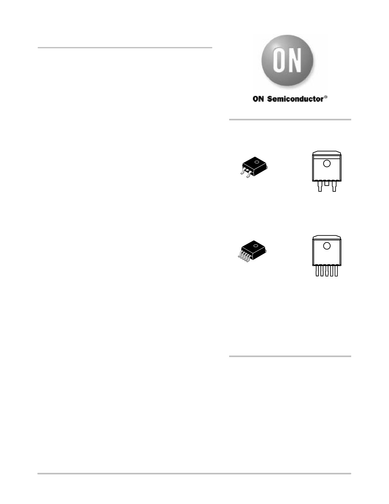
MARKING
DIAGRAMS
1
23
D2PAK
CASE 936
FIXED
NC
P565D2Txx
AWLYWWG
Tab = Ground
Pin 1. Vin
2. Ground
3. Vout
1
5
D2PAK
CASE 936A
ADJUSTABLE
NC
P565D2Txx
AWLYWWG
Tab = Ground
Pin 1. N.C.
2. Vin
3. Ground
4. Vout
5. Adj
xx = R4 or 12
A = Assembly Location
WL = Wafer Lot
Y = Year
WW = Work Week
G = Pb−Free
ORDERING INFORMATION
See detailed ordering and shipping information in the package
dimensions section on page 3 of this data sheet.
© Semiconductor Components Industries, LLC, 2004
July, 2004 − Rev. 8
1
Publication Order Number:
NCP565/D
1 page 
NCP565
TYPICAL CHARACTERISTICS
10 10
00
−10 −10
−20
Vin = 4.59 V
−20
Vin = 4.59 V
−30
Vout = 0.9 V
−30
Vout = 0.9 V
−40 −40
1.50
1.00
0.50
0 0 50 100 150 200 250 300 350 400
TIME (nS)
Figure 9. Load Transient from 10 mA to 1.5 A
1.50
1.00
0.50
0 0 0.5 1.0 1.5 2.0 2.5 3.0 3.5 4.0
TIME (ms)
Figure 10. Load Transient from 10 mA to 1.5 A
50
40
30 Vin = 4.59 V
20 Vout = 0.9 V
10
0
1.50
1.00
0.50
0
−50
0
50
100 150 200 250 300 350 400
TIME (nS)
Figure 11. Load Transient from 1.5 A to 10 mA
50
40
30 Vin = 4.59 V
20 Vout = 0.9 V
10
0
1.50
1.00
0.50
00 0.2 0.4 0.6 0.8 1.0 1.2 1.4 1.6
TIME (ms)
Figure 12. Load Transient from 1.5 A to 10 mA
100
90
80
70
60
50 Vin = 3.0 V
40
Vout = 0.9 V
Iout = 10 mA
30
20
10
0
Start 1.0 kHz
FREQUENCY (kHz)
Stop 100 kHz
Figure 13. Noise Density vs. Frequency
100
90
80
70
60 Vin = 3.0 V
50
Vout = 0.9 V
Iout = 1.5 A
40
30
20
10
0
Start 1.0 kHz
FREQUENCY (kHz)
Stop 100 kHz
Figure 14. Noise Density vs. Frequency
http://onsemi.com
5
5 Page 
NCP565
PACKAGE DIMENSIONS
D2PAK−5
D2T SUFFIX
CASE 936A−02
ISSUE B
−T−
A
OPTIONAL
CHAMFER
E
TERMINAL 6
U
KS
BH
1 2345
D
0.010 (0.254) M T
G
V
ML
NP
R
C
NOTES:
1. DIMENSIONING AND TOLERANCING PER ANSI
Y14.5M, 1982.
2. CONTROLLING DIMENSION: INCH.
3. TAB CONTOUR OPTIONAL WITHIN DIMENSIONS A
AND K.
4. DIMENSIONS U AND V ESTABLISH A MINIMUM
MOUNTING SURFACE FOR TERMINAL 6.
5. DIMENSIONS A AND B DO NOT INCLUDE MOLD
FLASH OR GATE PROTRUSIONS. MOLD FLASH
AND GATE PROTRUSIONS NOT TO EXCEED 0.025
(0.635) MAXIMUM.
INCHES
MILLIMETERS
DIM MIN MAX MIN MAX
A 0.386 0.403 9.804 10.236
B 0.356 0.368 9.042 9.347
C 0.170 0.180 4.318 4.572
D 0.026 0.036 0.660 0.914
E 0.045 0.055 1.143 1.397
G 0.067 BSC
1.702 BSC
H 0.539 0.579 13.691 14.707
K 0.050 REF
1.270 REF
L 0.000 0.010 0.000 0.254
M 0.088 0.102 2.235 2.591
N 0.018 0.026 0.457 0.660
P 0.058 0.078 1.473 1.981
R 5 _REF
5_ REF
S 0.116 REF
2.946 REF
U 0.200 MIN
5.080 MIN
V 0.250 MIN
6.350 MIN
SOLDERING FOOTPRINT*
8.38
0.33
10.66
0.42
1.702
0.067
16.02
0.63
1.016
3.05 0.04
0.12
ǒ ǓSCALE 3:1
mm
inches
*For additional information on our Pb−Free strategy and soldering
details, please download the ON Semiconductor Soldering and
Mounting Techniques Reference Manual, SOLDERRM/D.
http://onsemi.com
11
11 Page | ||
| Páginas | Total 12 Páginas | |
| PDF Descargar | [ Datasheet NCP565.PDF ] | |
Hoja de datos destacado
| Número de pieza | Descripción | Fabricantes |
| NCP5602 | High Efficiency Ultra Small Thinnest White LED Driver | ON Semiconductor |
| NCP5603 | High Efficiency Charge Pump Converter | ON Semiconductor |
| NCP5604A | High Efficiency White LED Driver | ON Semiconductor |
| NCP5604B | High Efficiency White LED Driver | ON Semiconductor |
| Número de pieza | Descripción | Fabricantes |
| SLA6805M | High Voltage 3 phase Motor Driver IC. |
Sanken |
| SDC1742 | 12- and 14-Bit Hybrid Synchro / Resolver-to-Digital Converters. |
Analog Devices |
|
DataSheet.es es una pagina web que funciona como un repositorio de manuales o hoja de datos de muchos de los productos más populares, |
| DataSheet.es | 2020 | Privacy Policy | Contacto | Buscar |