|
|
|
PDF NTD20N03L27G Data sheet ( Hoja de datos )
| Número de pieza | NTD20N03L27G | |
| Descripción | Power MOSFET ( Transistor ) | |
| Fabricantes | ON | |
| Logotipo | ||
Hay una vista previa y un enlace de descarga de NTD20N03L27G (archivo pdf) en la parte inferior de esta página. Total 6 Páginas | ||
|
No Preview Available !
NTD20N03L27
Power MOSFET
20 Amps, 30 Volts, N−Channel DPAK
This logic level vertical power MOSFET is a general purpose part
that provides the “best of design” available today in a low cost power
package. Avalanche energy issues make this part an ideal design in.
The drain−to−source diode has a ideal fast but soft recovery.
Features
• Pb−Free Packages are Available
• Ultra−Low RDS(on), Single Base, Advanced Technology
• SPICE Parameters Available
• Diode is Characterized for use in Bridge Circuits
• IDSS and VDS(on) Specified at Elevated Temperatures
• High Avalanche Energy Specified
• ESD JEDAC rated HBM Class 1, MM Class A, CDM Class 0
Typical Applications
• Power Supplies
• Inductive Loads
• PWM Motor Controls
• Replaces MTD20N03L in many Applications
MAXIMUM RATINGS (TC = 25°C unless otherwise noted)
Rating
Symbol Value Unit
Drain−to−Source Voltage
Drain−to−Gate Voltage (RGS = 1.0 MW)
Gate−to−Source Voltage
− Continuous
− Non−Repetitive (tpv10 ms)
Drain Current
− Continuous @ TA = 25_C
− Continuous @ TA = 100_C
− Single Pulse (tpv10 ms)
Total Power Dissipation @ TA = 25_C
Derate above 25°C
Total Power Dissipation @ TC = 25°C (Note 1)
VDSS
VDGR
VGS
VGS
ID
ID
IDM
PD
30
30
"20
"24
Vdc
Vdc
Vdc
20 Adc
16
60 Apk
74 W
0.6 W/°C
1.75 W
Operating and Storage Temperature Range
TJ, Tstg
−55 to
150
°C
Single Pulse Drain−to−Source Avalanche
Energy − Starting TJ = 25°C
(VDD = 30 Vdc, VGS = 5 Vdc, L = 1.0 mH,
IL(pk) = 24 A, VDS = 34 Vdc)
Thermal Resistance
− Junction−to−Case
− Junction−to−Ambient
− Junction−to−Ambient (Note 1)
Maximum Lead Temperature for Soldering
Purposes, 1/8″ from case for 10 seconds
EAS 288 mJ
RqJC
RqJA
RqJA
TL
°C/W
1.67
100
71.4
260 °C
Maximum ratings are those values beyond which device damage can occur.
Maximum ratings applied to the device are individual stress limit values (not
normal operating conditions) and are not valid simultaneously. If these limits
are exceeded, device functional operation is not implied, damage may occur
and reliability may be affected.
1. When surface mounted to an FR4 board using the minimum recommended
pad size and repetitive rating; pulse width limited by maximum junction
temperature.
© Semiconductor Components Industries, LLC, 2004
August, 2004 − Rev. 2
1
http://onsemi.com
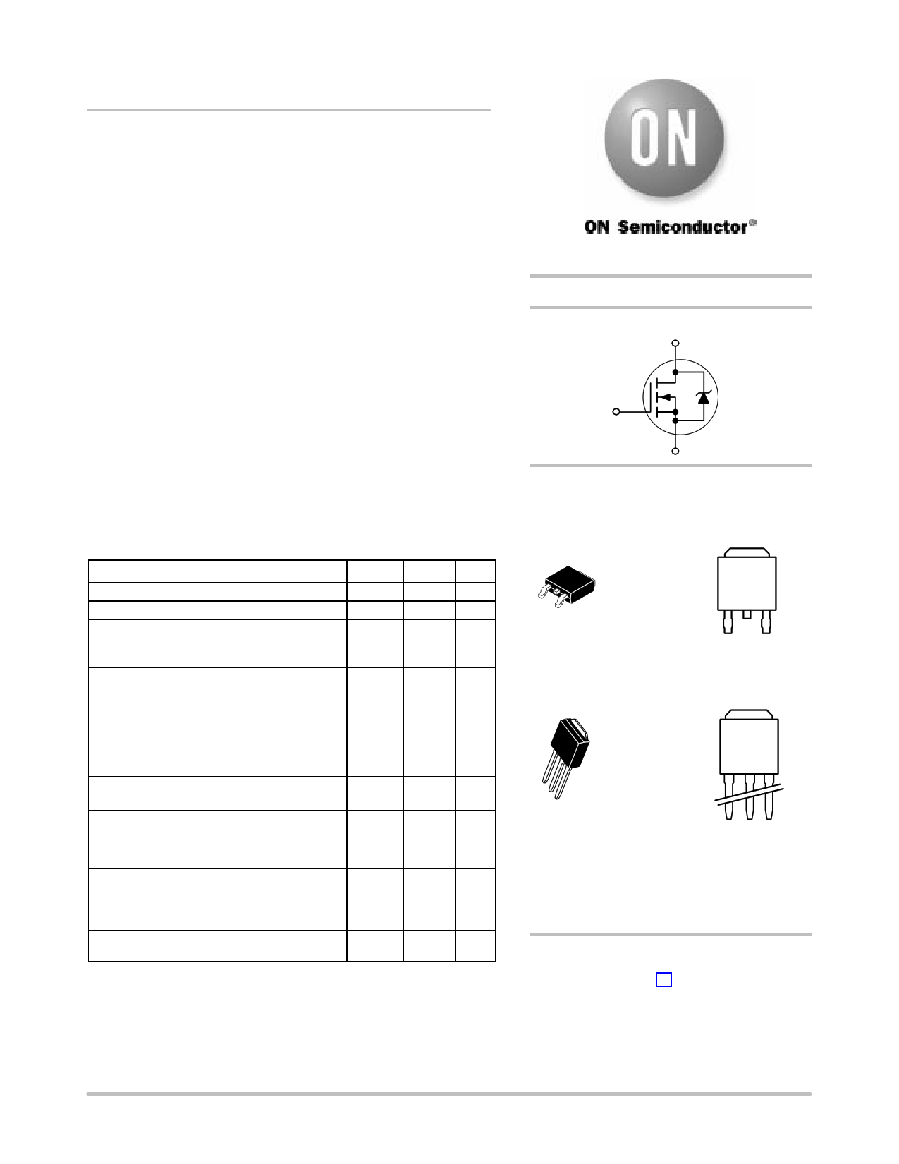
20 A, 30 V, RDS(on) = 27 mW
N−Channel
D
G
4
12
3
S
MARKING
DIAGRAMS
4
Drain
DPAK
CASE 369C
STYLE 2
1
Gate
2
Drain
3
Source
4
1
2
3
DPAK−3
CASE 369D
STYLE 2
4
Drain
12 3
Gate Drain Source
20N3L
A
Y
WW
= Device Code
= Assembly Location
= Year
= Work Week
ORDERING INFORMATION
See detailed ordering and shipping information in the package
dimensions section on page 2 of this data sheet.
Publication Order Number:
NTD20N03L27/D
1 page 
NTD20N03L27
PACKAGE DIMENSIONS
B
VR
DPAK
CASE 369C−01
ISSUE O
−T−
SEATING
PLANE
C
E
S
F
4
1 23
A
K
J
LH
D 2 PL
G 0.13 (0.005) M T
U
Z
SOLDERING FOOTPRINT*
6.20
0.244
2.58
0.101
3.0
0.118
5.80
0.228
1.6 6.172
0.063 0.243
INCHES
DIM MIN MAX
A 0.235 0.245
B 0.250 0.265
C 0.086 0.094
D 0.027 0.035
E 0.018 0.023
F 0.037 0.045
G 0.180 BSC
H 0.034 0.040
J 0.018 0.023
K 0.102 0.114
L 0.090 BSC
R 0.180 0.215
S 0.025 0.040
U 0.020 −−−
V 0.035 0.050
Z 0.155 −−−
STYLE 2:
PIN 1. GATE
2. DRAIN
3. SOURCE
4. DRAIN
MILLIMETERS
MIN MAX
5.97 6.22
6.35 6.73
2.19 2.38
0.69 0.88
0.46 0.58
0.94 1.14
4.58 BSC
0.87 1.01
0.46 0.58
2.60 2.89
2.29 BSC
4.57 5.45
0.63 1.01
0.51 −−−
0.89 1.27
3.93 −−−
ǒ ǓSCALE 3:1
mm
inches
*For additional information on our Pb−Free strategy and soldering
details, please download the ON Semiconductor Soldering and
Mounting Techniques Reference Manual, SOLDERRM/D.
http://onsemi.com
5
5 Page | ||
| Páginas | Total 6 Páginas | |
| PDF Descargar | [ Datasheet NTD20N03L27G.PDF ] | |
Hoja de datos destacado
| Número de pieza | Descripción | Fabricantes |
| NTD20N03L27 | Power MOSFET ( Transistor ) | ON |
| NTD20N03L27G | Power MOSFET ( Transistor ) | ON |
| NTD20N03L27T4 | Power MOSFET ( Transistor ) | ON |
| NTD20N03L27T4G | Power MOSFET ( Transistor ) | ON |
| Número de pieza | Descripción | Fabricantes |
| SLA6805M | High Voltage 3 phase Motor Driver IC. |
Sanken |
| SDC1742 | 12- and 14-Bit Hybrid Synchro / Resolver-to-Digital Converters. |
Analog Devices |
|
DataSheet.es es una pagina web que funciona como un repositorio de manuales o hoja de datos de muchos de los productos más populares, |
| DataSheet.es | 2020 | Privacy Policy | Contacto | Buscar |