|
|
|
PDF NM34W02 Data sheet ( Hoja de datos )
| Número de pieza | NM34W02 | |
| Descripción | 2K-Bit Standard 2-Wire Bus Interface Serial EEPROM with Full Array Write Protect | |
| Fabricantes | Fairchild | |
| Logotipo | ||
Hay una vista previa y un enlace de descarga de NM34W02 (archivo pdf) en la parte inferior de esta página. Total 12 Páginas | ||
|
No Preview Available !
March 1999
NM34W02
2K-Bit Standard 2-Wire Bus Interface Serial EEPROM
with Full Array Write Protect
Designed with Permanent Write-Protection for First 128 Bytes for Serial Presence
Detect Application on Memory Modules (PC100 Compliant)
General Description
The NM34W02 is 2048 bits of CMOS non-volatile electrically
erasable memory. This device is specifically designed to support
Serial Presence Detect circuitry in memory modules. This com-
munications protocol uses CLOCK (SCL) and DATA I/O (SDA)
lines to synchronously clock data between the master (for ex-
ample a microprocessor) and the slave EEPROM device(s).
The contents of the non-volatile memory allows the CPU to
determine the capacity of the module and the electrical character-
istics of the memory devices it contains. This will enable "plug and
play" capability as the module is read and PC main memory
resources utilized through the memory controller.
The first 128 bytes of the memory of the NM34W02 can be
permanently Write Protected by writing to the "WRITE PROTECT"
Register. Write Protect implementation details are described
under the section titled Addressing the WP Register. In addition,
like the NM24Wxx product family, the entire memory array can be
write-protected through "WP" pin.
The NM34W02 is available in a JEDEC standard TSSOP package
for low profile memory modules for systems requiring efficient
space utilization such as in a notebook computer. Two options are
available: L - Low Voltage and LZ - Low Power, allowing the part
to be used in systems where battery life is of primary importance.
Features
s PC100 Compliant
s Extended Operating Voltage: 2.7V-5.5V
s Software Write-Protection for first 128 bytes
s Hardware Write-Protection for entire memory array
s 200 µA active current typical
– 1.0 µA standby current typical (L)
– 0.1 µA standby current typical (LZ)
s IIC compatible interface
– Provides bidirectional data transfer protocol
s Sixteen byte page write mode
– Minimizes total write time per byte
s Self timed write cycle
- Typical write cycle time of 6ms
s Endurance: 1,000,000 data changes
s Data retention greater than 40 years
s Packages available: 8-pin TSSOP and 8-pin SO
s Temperature Ranges: Commercial and Extended
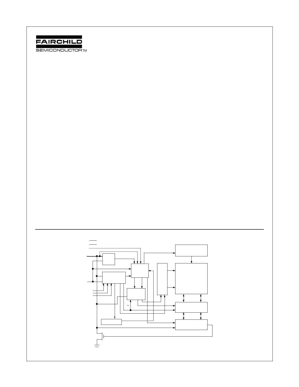
Block Diagram
VCC
VSS
WP
SDA
SCL
A2
A1
A0
START
STOP
LOGIC
START CYCLE
H.V. GENERATION
TIMING &CONTROL
SLAVE ADDRESS
REGISTER &
COMPARATOR
CONTROL
LOGIC
LOAD
INC
WORD
ADDRESS
COUNTER
R/W
XDEC
16
E2PROM
ARRAY
16 x 16 x 8
0/1/2/3
4
4
16
YDEC
Write Protect
Register
Device Address Bits
DIN
8
CK
DATA REGISTER
DOUT
© 1999 Fairchild Semiconductor Corporation
NM34W02 Rev. C.2
1
DS500078-1
www.fairchildsemi.com
1 page 
Bus Timing
tF
tHIGH
tLOW
SCL
SDA
tSU:STA
tHD:STA
,,IN
SDA
OUT
tAA
Background Information (IIC Bus)
tHD:DAT
As mentioned, the IIC bus allows synchronous bidirectional com-
munication between Transmitter/Receiver using the SCL (clock)
and SDA (Data I/O) lines. All communication must be started with
a valid START condition, concluded with a STOP condition and
acknowledged by the Receiver with an ACKNOWLEDGE condi-
tion.
In addition, since the IIC bus is designed to support other devices
such as RAM, EPROMs, etc., a device type identifier string must
follow the START condition. For EEPROMs, this 4-bit string is
1010. Also refer the Addressing the WP Register section.
As shown below, although the EEPROMs on the IIC bus may be
configured in any manner required, the total memory addressed
can not exceed 16K (16,384 bits) on the Standard IIC. EEPROM
memory address programming is controlled by 2 methods:
• Hardware configuring the A0, A1, and A2 pins (Device
Address pins) with pull-up or pull-down to VCC or VSS. All
unused pins must be grounded (tied to VSS).
• Software addressing the required PAGE BLOCK within the
device memory array (as sent in the Slave Address string).
Addressing an EEPROM memory location involves sending a
command string with the following information:
tR
tLOW
tSU:DAT
tSU:STO
tDH
tBUF
DS500078-5
BYTE
PAGE
PAGE BLOCK
MASTER
SLAVE
TRANSMITTER
RECEIVER
DEFINITIONS
8 bits of data
16 sequential addresses (one byte
each) that may be programmed
during a 'Page Write' programming
cycle
2,048 (2K) bits organized into 16
pages of addressable memory. (8
bits) x (16 bytes) x (16 pages) = 2,048
bits
Any IIC device CONTROLLING the
transfer of data (such as a micropro-
cessor)
Device being controlled (EEPROMs
are always considered Slaves)
Device currently SENDING data on
the bus (may be either a Master or
Slave).
Device currently receiving data on the
bus (Master or Slave)
[DEVICE TYPE]—[DEVICE ADDRESS]—[PAGE BLOCK
ADDRESS]—[BYTE ADDRESS]
Example of 16K of Memory on 2-Wire Bus
VCC
VCC
SDA
SCL
VCC
VCC
VCC
VCC
NM34C02L
A0 A1 A2 VSS
NM24C02
A0 A1 A2 VSS
NM24C04
A0 A1 A2 VSS
NM24C08
A0 A1 A2 VSS
To VCC or VSS
To VCC or VSS
To VCC or VSS
Note:
The SDA pull-up resistor is required due to the open-drain/open collector output of IIC bus devices.
The SCL pull-up resistor is recommended because of the normal SCL line inactive 'high' state.
It is recommended that the total line capacitance be less than 400pF.
Specific timing and addressing considerations are described in greater detail in the following sections.
To VCC or VSS
DS500078-6
NM34W02 Rev. C.2
5 www.fairchildsemi.com
5 Page 
Physical Dimensions inches (millimeters) unless otherwise noted
0.189 - 0.197
(4.800 - 5.004)
87 65
0.228 - 0.244
(5.791 - 6.198)
0.010 - 0.020 x 45°
(0.254 - 0.508)
0.150 - 0.157
(3.810 - 3.988)
8° Max, Typ.
All leads
0.0075 - 0.0098
(0.190 - 0.249)
Typ. All Leads
0.04
(0.102)
All lead tips
0.016 - 0.050
(0.406 - 1.270)
Typ. All Leads
12 34
Lead #1
IDENT
0.053 - 0.069
(1.346 - 1.753)
0.014
(0.356)
0.050
(1.270)
Typ
0.004 - 0.010
(0.102 - 0.254)
Seating
Plane
0.014 - 0.020 Typ.
(0.356 - 0.508)
8-Pin Molded Small Outline Package (M8)
Order Number NM34W02LM8/LZM8
Package Number M08A
NM34W02 Rev. C.2
11 www.fairchildsemi.com
11 Page | ||
| Páginas | Total 12 Páginas | |
| PDF Descargar | [ Datasheet NM34W02.PDF ] | |
Hoja de datos destacado
| Número de pieza | Descripción | Fabricantes |
| NM34W02 | 2K-Bit Standard 2-Wire Bus Interface Serial EEPROM with Full Array Write Protect | Fairchild |
| Número de pieza | Descripción | Fabricantes |
| SLA6805M | High Voltage 3 phase Motor Driver IC. |
Sanken |
| SDC1742 | 12- and 14-Bit Hybrid Synchro / Resolver-to-Digital Converters. |
Analog Devices |
|
DataSheet.es es una pagina web que funciona como un repositorio de manuales o hoja de datos de muchos de los productos más populares, |
| DataSheet.es | 2020 | Privacy Policy | Contacto | Buscar |