|
|
|
PDF 82C55 Data sheet ( Hoja de datos )
| Número de pieza | 82C55 | |
| Descripción | CMOS Programmable peripheral Interface | |
| Fabricantes | Wing Shing Computer Components | |
| Logotipo | ||
Hay una vista previa y un enlace de descarga de 82C55 (archivo pdf) en la parte inferior de esta página. Total 25 Páginas | ||
|
No Preview Available !
CMOS Programmable peripheral
Interface
WS82C55A
Features
Description
• Pin Compatible with NMOS 8255A
• 24 Programmable I/O Pins
• Fully TTL Compatible
• High Speed, No “Wait State” Operation with 5MHz
80C86 and 8MHz 80C88
• Direct Bit Set/Reset Capability
• Enhanced Control Word Read Capability
• L7 Process
• 2.5mA Drive Capability on All I/O Ports
• Low Standby Power (ICCSB) . . . . . . . . . . . . . . . . .10µA
Ordering Information
The WS82C55A is a high performance CMOS version of
the industry standard 8255A and is manufactured using a
self-aligned silicon gate CMOS process (Scaled SAJI IV). It
is a general purpose programmable I/O device which may be
used with many different microprocessors. There are 24 I/O
pins which may be individually programmed in 2 groups of
12 and used in 3 major modes of operation. The high
performance and industry standard configuration of the
WS82C55A make it compatible with the 80C86, and
other microprocessors.
Static CMOS circuit design insures low operating power. TTL
compatibility over the full military temperature range and bus
hold circuitry eliminate the need for pull-up resistors. The
advanced SAJI process results in performance equal
to or greater than existing functionally equivalent products at
a fraction of the power.
PART NUMBERS
WS82C55A-5P
WS82C55A-5C
WS82C55A-5Q
SPEED
5MHz
5MHz
5MHz
PART NUMBERS
WS82C55AP
WS82C55AC
WS82C55AQ
SPEED
8MHz
8MHz
8MHz
TEMPERATURE
RANGE
PKG.
oo
0 C to 70 C
40DIP
oo
0 C to 70 C
44 PLCC
oo
0 C to 70 C
44 QFP
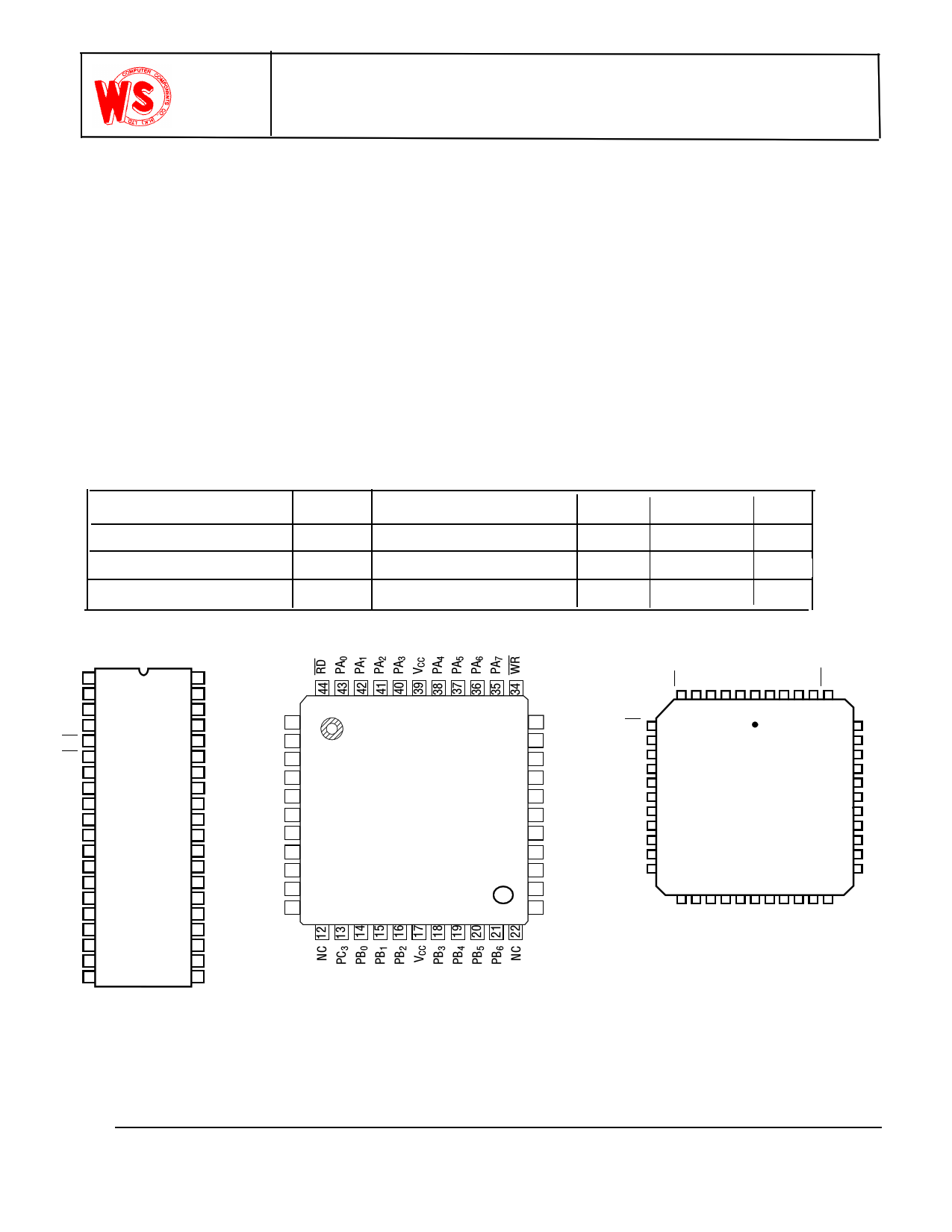
Pinouts
PA3 1
40 PA4
PA2 2
39 PA5
PA1 3
38 PA6
PA0 4
37 PA7
RD 5
36 WR
CS 6
35 RESET
GND 7 WS82C55A-5P 34 D0
A1 8 WS82C55AP 33 D1
A0 9
32 D2
PC7 10
31 D3
PC6 11
30 D4
PC5 12
29 D5
PC4 13 DIP-40
PC0 14
28 D6
27 D7
PC1 15
PC2 16
26 VCC
25 PB7
PC3 17
24 PB6
PB0 18
23 PB5
PB1 19
22 PB4
PB2 20
21 PB3
CS
GND
A1
A0
PC7
PC6
PC5
PC4
PC0
PC1
PC2
1
2
3
4
5
6
7
8
9
10
11
WS82C55A-5Q
WS82C55AQ
QFP-44
33 RESET
32 D0
31 D1
30 D2.
29 D3
28 D4
27 D5
26 D6
25 D7
24 VCC
23 PB7
CS
GND
A1
A0
PC7
NC
PC6
PC5
PC4
PC0
PC1
6 5 4 3 2 1 44 43 42 41 40
7 39
8 38
9
WS82C55A-5C
37
10 WS82C55AC 36
11 35
12 34
13 33
14
PLCC-44
32
15 31
16 30
17 29
18 1920 21 22 23 24 25 26 27 28
RESET
D0
D1
D2
D3
NC
D4
D5
D6
D7
VCC
CAUTION: These devices are sensitive to electrostatic discharge; follow proper IC Handling Procedures.
Wing Shing Computer Components Co., (H.K.)Ltd.
Homepage: http://www.wingshing.com
1
Tel:(852)2341 9276 Fax:(852)2797 8153
E-mail: [email protected]
1 page 
WS82C55A
The modes for Port A and Port B can be separately defined,
while Port C is divided into two portions as required by the
Port A and Port B definitions. All of the output registers,
including the status flip-flops, will be reset whenever the
mode is changed. Modes may be combined so that their
functional definition can be “tailored” to almost any I/O
structure. For instance: Group B can be programmed in
Mode 0 to monitor simple switch closings or display compu-
tational results, Group A could be programmed in Mode 1 to
monitor a keyboard or tape reader on an interrupt-driven
basis.
The mode definitions and possible mode combinations may
seem confusing at first, but after a cursory review of the
complete device operation a simple, logical I/O approach will
surface. The design of the 82C55A has taken into account
things such as efficient PC board layout, control signal defi-
nition vs. PC layout and complete functional flexibility to sup-
port almost any peripheral device with no external logic.
Such design represents the maximum use of the available
pins.
Single Bit Set/Reset Feature (Figure 5)
Any of the eight bits of Port C can be Set or Reset using a
single Output instruction. This feature reduces software
requirements in control-based applications.
When Port C is being used as status/control for Port A or B,
these bits can be set or reset by using the Bit Set/Reset
operation just as if they were output ports.
This function allows the programmer to enable or disable a
CPU interrupt by a specific I/O device without affecting any
other device in the interrupt structure.
INTE Flip-Flop Definition
(BIT-SET)-INTE is SET - Interrupt Enable
(BIT-RESET)-INTE is Reset - Interrupt Disable
NOTE: All Mask flip-flops are automatically reset during mode se-
lection and device Reset.
Operating Modes
Mode 0 (Basic Input/Output). This functional configuration
provides simple input and output operations for each of the
three ports. No handshaking is required, data is simply writ-
ten to or read from a specific port.
Mode 0 Basic Functional Definitions:
• Two 8-bit ports and two 4-bit ports
• Any Port can be input or output
• Outputs are latched
• Input are not latched
• 16 different Input/Output configurations possible
MODE 0 PORT DEFINITION
A B GROUP A
GROUP B
CONTROL WORD
D7 D6 D5 D4 D3 D2 D1 D0
XX X
DON’T
CARE
BIT SET/RESET
1 = SET
0 = RESET
BIT SELECT
01234567
0 1 0 1 0 1 0 1 B0
0 0 1 1 0 0 1 1 B1
0 0 0 0 1 1 1 1 B2
D4 D3
00
00
00
00
01
01
01
D1
0
0
1
1
0
0
1
PORT C
PORT C
D0 PORT A (Upper) # PORT B (Lower)
0 Output Output 0 Output Output
1 Output Output 1 Output Input
0 Output Output 2 Input Output
1 Output Output 3 Input Input
0 Output Input 4 Output Output
1 Output Input 5 Output Input
0 Output Input 6 Input Output
BIT SET/RESET FLAG
0 = ACTIVE
01 1
10 0
1 Output Input 7 Input Input
0 Input Output 8 Output Output
FIGURE 5. BIT SET/RESET FORMAT
1 0 0 1 Input Output 9 Output Input
Interrupt Control Functions
1 0 1 0 Input Output 10 Input Output
1 0 1 1 Input Output 11 Input Input
When WS82C55A is programmed to operate in mode 1 or
mode 2, control signals are provided that can be used as 1 1 0 0 Input Input 12 Output Output
interrupt request inputs to the CPU. The interrupt request
signals, generated from port C, can be inhibited or enabled
by setting or resetting the associated INTE flip-flop, using the
11 0
11 1
1 Input Input 13 Output Input
0 Input Input 14 Input Output
bit set/reset function of port C.
1 1 1 1 Input Input 15 Input Input
5
5 Page 
CONTROL WORD
D7 D6 D5 D4 D3 D2 D1 D0
11
1/0 1/0 1/0
PC2-PC0
1 = INPUT
0 = OUTPUT
PORT B
1 = INPUT
0 = OUTPUT
GROUP B MODE
0 = MODE 0
1 = MODE 1
FIGURE 11. MODE CONTROL WORD
WS82C55A
PC3
INTRA
PA7-PA0 8
INTE
1
PC7
PC6
OBFA
ACKA
INTE
2
PC4
STBA
PC5
IBFA
WR
RD PC2-PC0 3 I/O
FIGURE 12. MODE 2
DATA FROM
CPU TO 82C55A
WR
OBF
INTR
ACK
STB
tWOB
tST
tAOB
tAK
IBF
PERIPHERAL
BUS
tSIB
tPS
tPH
tAD tKD
tRIB
RD
DATA FROM
DATA FROM
PERIPHERAL TO WS82C55A
WS82C55A TO PERIPHERAL
DATA FROM
WS82C55A TO CPU
NOTE: Any sequence where WR occurs before ACK and STB occurs before RD is permissible. (INTR = IBF • MASK • STB • RD ÷ OBF •
MASK • ACK • WR)
FIGURE 13. MODE 2 (BI-DIRECTIONAL)
11
11 Page | ||
| Páginas | Total 25 Páginas | |
| PDF Descargar | [ Datasheet 82C55.PDF ] | |
Hoja de datos destacado
| Número de pieza | Descripción | Fabricantes |
| 82C50 | CMOS Asynchronous Communications Element | Intersil Corporation |
| 82C50 | VOLTAGE DETECTORS | Unisonic Technologies |
| 82C501 | Ethernet Serial Interface | Intel |
| 82C50A | CMOS Asynchronous Communications Element | Intersil Corporation |
| Número de pieza | Descripción | Fabricantes |
| SLA6805M | High Voltage 3 phase Motor Driver IC. |
Sanken |
| SDC1742 | 12- and 14-Bit Hybrid Synchro / Resolver-to-Digital Converters. |
Analog Devices |
|
DataSheet.es es una pagina web que funciona como un repositorio de manuales o hoja de datos de muchos de los productos más populares, |
| DataSheet.es | 2020 | Privacy Policy | Contacto | Buscar |