|
|
|
PDF MAX1651 Data sheet ( Hoja de datos )
| Número de pieza | MAX1651 | |
| Descripción | 5V/3.3V or Adjustable / High-Efficiency / Low-Dropout / Step-Down DC-DC Controllers | |
| Fabricantes | Maxim Integrated | |
| Logotipo | ||
Hay una vista previa y un enlace de descarga de MAX1651 (archivo pdf) en la parte inferior de esta página. Total 12 Páginas | ||
|
No Preview Available !
19-0305; Rev 2; 9/95
5V/3.3V or Adjustable, High-Efficiency,
Low-Dropout, Step-Down DC-DC Controllers
_______________General Description
The MAX1649/MAX1651 BiCMOS, step-down, DC-DC
switching controllers provide high efficiency over loads
ranging from 1mA to more than 2.5A. A unique, current-
limited pulse-frequency-modulated (PFM) control scheme
gives these devices the benefits of pulse-width-modula-
tion (PWM) converters (high efficiency at heavy loads),
while using only 100µA of supply current (vs. 2mA to
10mA for PWM converters). Dropout performance down
to 300mV is provided by a high switch duty cycle (96.5%)
and a low current-sense threshold (110mV).
A high switching frequency (up to 300kHz) allows these
devices to use miniature external components.
The MAX1649/MAX1651 have dropout voltages less
than 0.3V at 500mA and accept input voltages up to
16V. Output voltages are preset at 5V (MAX1649), or
3.3V (MAX1651). They can also be adjusted to any
voltage from 1.5V to the input voltage by using two
resistors.
These step-down controllers drive external P-channel
MOSFETs at loads greater than 12.5W. If less power is
required, use the MAX639/MAX640/MAX653 step-down
converters with on-chip FETs, which allow up to a
225mA load current.
________________________Applications
PDAs
High-Efficiency Step-Down Regulation
5V-to-3.3V Green PC Applications
Battery-Powered Applications
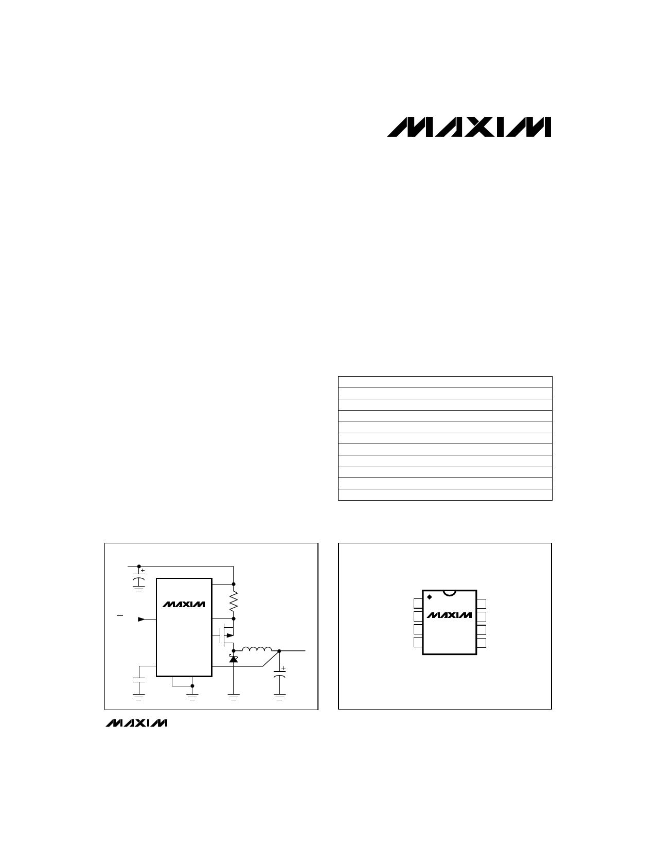
__________Typical Operating Circuit
INPUT
3.6V TO 16V
____________________________Features
o More than 90% Efficiency (10mA to 1.5A Loads)
o More than 12.5W Output Power
o Less than 0.3V Dropout Voltage at 500mA
o 100µA Max Quiescent Supply Current
o 5µA Max Shutdown Supply Current
o 16V Max Input Voltage
o 5V (MAX1649), 3.3V (MAX1651), or Adjustable
Output Voltage
o Current-Limited Control Scheme
o Up to 300kHz Switching Frequency
o Up to 96.5% Duty Cycle
______________Ordering Information
PART
TEMP. RANGE
MAX1649CPA
0°C to +70°C
MAX1649CSA
0°C to +70°C
MAX1649C/D
0°C to +70°C
MAX1649EPA
-40°C to +85°C
MAX1649ESA
-40°C to +85°C
MAX1651CPA
0°C to +70°C
MAX1651CSA
0°C to +70°C
MAX1651C/D
0°C to +70°C
MAX1651EPA
-40°C to +85°C
MAX1651ESA
-40°C to +85°C
* Dice are tested at TA = +25°C.
PIN-PACKAGE
8 Plastic DIP
8 SO
Dice*
8 Plastic DIP
8 SO
8 Plastic DIP
8 SO
Dice*
8 Plastic DIP
8 SO
__________________Pin Configuration
TOP VIEW
ON/OFF
V+
MAX1651
SHDN
CS
EXT
REF OUT
FB GND
P
OUTPUT
3.3V
OUT 1
FB 2
SHDN 3
REF 4
MAX1649
MAX1651
8 GND
7 EXT
6 CS
5 V+
DIP/SO
________________________________________________________________ Maxim Integrated Products 1
Call toll free 1-800-998-8800 for free samples or literature.
1 page 
5V/3.3V or Adjustable, High-Efficiency,
Low-Dropout, Step-Down DC-DC Controllers
____________________________Typical Operating Characteristics (continued)
(TA = +25°C, unless otherwise noted.)
MAX1649
LINE-TRANSIENT RESPONSE
MAX1649
LOAD-TRANSIENT RESPONSE
A
5ms/div
CIRCUIT OF FIGURE 1, ILOAD = 1A
A: VOUT = 5V, 100mV/div, AC-COUPLED
B: V+ = 6V TO 16V, 5V/div
16V
B
6V
MAX1649
SHDN RESPONSE TIME
1ms/div
CIRCUIT OF FIGURE 1, V+ = 10V, ILOAD = 1A
200µs/div
CIRCUIT OF FIGURE 1, V+ = 10V
A: VOUT = 5V, 100mV/div, AC-COUPLED
B: ILOAD = 30mA TO 1.6A, 1A/div
5V
OUTPUT
0V
4V
SHDN
INPUT
0V
A
1.6A
B
0A
_______________________________________________________________________________________ 5
5 Page 
5V/3.3V or Adjustable, High-Efficiency,
Low-Dropout, Step-Down DC-DC Controllers
Table 2. Component Suppliers
COMPANY
AVX USA
Coiltronics
CoilCraft
Dale
International
Rectifier
IRC
USA
USA
USA
USA
USA
Motorola
USA
Nichicon
Nihon
Sanyo
USA
Japan
USA
Japan
USA
Japan
Siliconix
USA
Sprague
Sumida
United
Chemi-Con
USA
USA
Japan
USA
PHONE
(207) 282-5111
or
(800) 282-4975
(407) 241-7876
(708) 639-6400
(402) 564-3131
(310) 322-3331
(512) 992-7900
(602) 244-3576
or
(602) 244-5303
(708) 843-7500
81-7-5231-8461
(805) 867-2555
81-3-3494-7411
(619) 661-6835
81-7-2070-6306
(408) 988-8000
or
(800) 554-5565
(603) 224-1961
(708) 956-0666
81-3-3607-5111
(714) 255-9500
FAX
(207) 283-1941
(407) 241-9339
(708) 639-1469
(402) 563-1841
(310) 322-3332
(512) 992-3377
(602) 244-4015
(708) 843-2798
81-7-5256-4158
(805) 867-2556
81-3-3494-7414
(619) 661-1055
81-7-2070-1174
(408) 970-3950
(603) 224-1430
(708) 956-0702
81-3-3607-5144
(714) 255-9400
Input Bypass Capacitor
The input bypass capacitor reduces peak currents
drawn from the voltage source, and also reduces the
amount of noise at the voltage source caused by the
switching action of the MAX1649/MAX1651. The input
voltage source impedance determines the size of the
capacitor required at the V+ input. As with the output fil-
ter capacitor, a low-ESR capacitor is recommended.
Bypass the IC separately with a 0.1µF ceramic capac-
itor placed close to the V+ and GND pins.
Reference Capacitor
Bypass REF with a 0.1µF or larger capacitor.
Layout Considerations
Proper PC board layout is essential because of high
current levels and fast switching waveforms that radi-
ate noise. Minimize ground noise by connecting the
anode of the rectifier, the input bypass capacitor
ground lead, and the output filter capacitor ground
lead to a single point (“star” ground configuration). A
ground plane is recommended. Also minimize lead
lengths to reduce stray capacitance, trace resistance,
and radiated noise. In particular, the traces connected
to FB (if an external resistor divider is used) and EXT
must be short. Place the 0.1µF ceramic bypass capac-
itor as close as possible to the V+ and GND pins.
MAX1649/MAX1651 vs. MAX649/MAX651
The MAX1649 and MAX1651 are pin compatible with
the MAX649 and MAX651, but have been optimized for
improved dropout performance and efficiency—partic-
ularly with low input voltages. The MAX1649/MAX1651
feature increased maximum switch duty cycle (96.5%)
and reduced current-limit sense voltage (110mV).
Their predecessors, the MAX649/MAX651, use a high-
er two-step (210mV/110mV) current-limit sense voltage
to provide tighter current-sense accuracy and reduced
inductor peak current at light loads.
___________________Chip Topography
OUT GND
FB
SHDN
EXT
0.106"
(2.692mm)
CS
REF V+
0.081"
(2.057mm)
TRANSISTOR COUNT: 428
SUBSTRATE CONNECTED TO V+
______________________________________________________________________________________ 11
11 Page | ||
| Páginas | Total 12 Páginas | |
| PDF Descargar | [ Datasheet MAX1651.PDF ] | |
Hoja de datos destacado
| Número de pieza | Descripción | Fabricantes |
| MAX165 | CMOS P-Compatible / 5s / 8-Bit ADCs | Maxim Integrated |
| MAX1651 | 5V/3.3V or Adjustable / High-Efficiency / Low-Dropout / Step-Down DC-DC Controllers | Maxim Integrated |
| MAX1652 | High-Efficiency / PWM / Step-Down DC-DC Controllers in 16-Pin QSOP | Maxim Integrated |
| MAX1652EEE | High-Efficiency / PWM / Step-Down DC-DC Controllers in 16-Pin QSOP | Maxim Integrated |
| Número de pieza | Descripción | Fabricantes |
| SLA6805M | High Voltage 3 phase Motor Driver IC. |
Sanken |
| SDC1742 | 12- and 14-Bit Hybrid Synchro / Resolver-to-Digital Converters. |
Analog Devices |
|
DataSheet.es es una pagina web que funciona como un repositorio de manuales o hoja de datos de muchos de los productos más populares, |
| DataSheet.es | 2020 | Privacy Policy | Contacto | Buscar |