|
|
|
PDF MAX1227 Data sheet ( Hoja de datos )
| Número de pieza | MAX1227 | |
| Descripción | 12-Bit 300ksps ADCs with FIFO / Temp Sensor / Internal Reference | |
| Fabricantes | Maxim Integrated | |
| Logotipo | ||
Hay una vista previa y un enlace de descarga de MAX1227 (archivo pdf) en la parte inferior de esta página. Total 24 Páginas | ||
|
No Preview Available !
19-2851; Rev 1; 7/03
EVAALVUAAILTAIOBNLEKIT
12-Bit 300ksps ADCs with FIFO,
Temp Sensor, Internal Reference
General Description
The MAX1227/MAX1229/MAX1231 are serial 12-bit ana-
log-to-digital converters (ADCs) with an internal reference
and an internal temperature sensor. These devices fea-
ture on-chip FIFO, scan mode, internal clock mode, inter-
nal averaging, and AutoShutdown™. The maximum
sampling rate is 300ksps using an external clock. The
MAX1231 has 16 input channels, the MAX1229 has 12
input channels, and the MAX1227 has 8 input channels.
All input channels are configurable for single-ended or
differential inputs in unipolar or bipolar mode. All three
devices operate from a +3V supply and contain a 10MHz
SPI™/QSPI™/MICROWIRE™-compatible serial port.
The MAX1231 is available in 28-pin 5mm x 5mm QFN
with exposed pad and 24-pin QSOP packages. The
MAX1227/MAX1229 are only available in QSOP pack-
ages. All three devices are specified over the extended
-40°C to +85°C temperature range.
________________________Applications
System Supervision
Data-Acquisition Systems
Industrial Control Systems
Patient Monitoring
Data Logging
Instrumentation
AutoShutdown is a trademark of Maxim Integrated Products, Inc.
SPI/QSPI are trademarks of Motorola, Inc.
MICROWIRE is a trademark of National Semiconductor Corp.
Features
o Internal Temperature Sensor (±1°C Accuracy)
o 16-Entry First-In/First-Out (FIFO)
o Analog Multiplexer with True Differential
Track/Hold
16-, 12-, 8-Channel Single Ended
8-, 6-, 4-Channel True Differential
(Unipolar or Bipolar)
o Accuracy: ±1 LSB INL, ±1 LSB DNL, No Missing
Codes Over Temperature
o Scan Mode, Internal Averaging, and Internal Clock
o Low-Power Single +3V Operation
0.62mA at 300ksps
o Internal 2.5V Reference or External Differential
Reference
o 10MHz 3-Wire SPI/QSPI/MICROWIRE-Compatible
Interface
o Space-Saving 28-Pin 5mm x 5mm QFN Package
Ordering Information
PART
TEMP RANGE
PIN-PACKAGE
MAX1227ACEE-T*
0°C to +70°C
16 QSOP
MAX1227AEEE-T* -40°C to +85°C
16 QSOP
*Future product—contact factory for availability.
Ordering Information continued at end of data sheet.
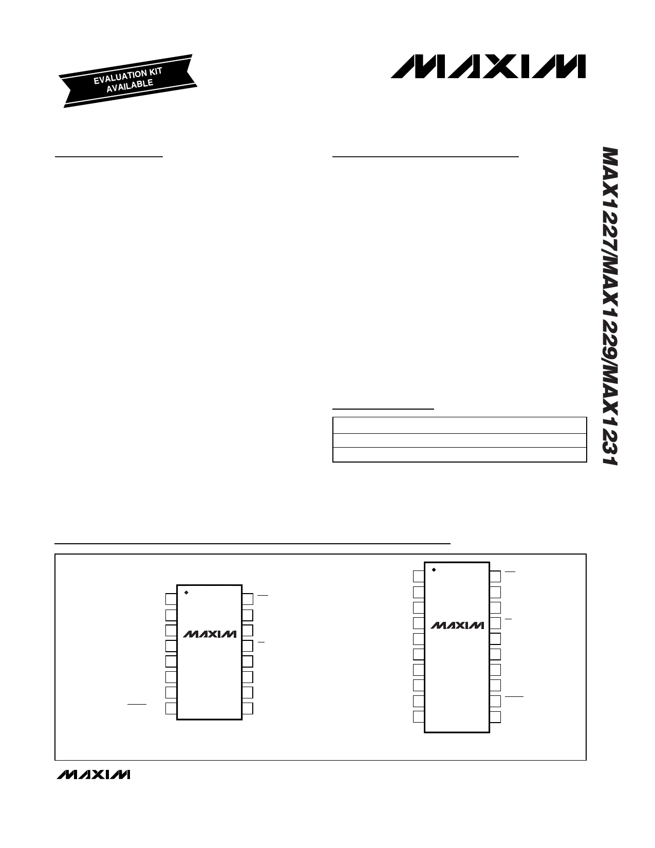
Pin Configurations
TOP VIEW
AIN0 1
AIN1 2
AIN2 3
AIN3 4
AIN4 5
AIN5 6
REF-/AIN6 7
CNVST/AIN7 8
MAX1227
16 EOC
15 DOUT
14 DIN
13 CS
12 SCLK
11 VDD
10 GND
9 REF+
QSOP
Pin Configurations continued at end of data sheet.
AIN0 1
AIN1 2
AIN2 3
AIN3 4
AIN4 5
AIN5 6
AIN6 7
AIN7 8
AIN8 9
AIN9 10
MAX1229
QSOP
20 EOC
19 DOUT
18 DIN
17 CS
16 SCLK
15 VDD
14 GND
13 REF+
12 CNVST/AIN11
11 REF-/AIN10
________________________________________________________________ Maxim Integrated Products 1
For pricing, delivery, and ordering information, please contact Maxim/Dallas Direct! at
1-888-629-4642, or visit Maxim’s website at www.maxim-ic.com.
1 page 
12-Bit 300ksps ADCs with FIFO,
Temp Sensor, Internal Reference
TIMING CHARACTERISTICS (Figure 1)
PARAMETER
SCLK Clock Period
SCLK Duty Cycle
SCLK Fall to DOUT Transition
CS Rise to DOUT Disable
CS Fall to DOUT Enable
DIN to SCLK Rise Setup
SCLK Rise to DIN Hold
CS to SCLK Rise Setup
SCLK Rise to CS Hold
CNVST Pulse Width
SYMBOL
tCP
tCH
tDOT
tDOD
tDOE
tDS
tDH
tCSS
tCSH
tCSW
CONDITIONS
Externally clocked conversion
Data I/O
CLOAD = 30pF
CLOAD = 30pF
CLOAD = 30pF
CKSEL = 00, CKSEL = 01 (temp sense)
CKSEL = 01 (voltage conversion)
MIN TYP MAX UNITS
208
ns
100
40 60 %
40 ns
40 ns
40 ns
40 ns
0 ns
40 ns
0 ns
40 ns
1.4 µs
CS or CNVST Rise to EOC
Low (Note 9)
tTS Temp sense
Voltage conversion
Reference power-up
55
7 µs
65
Note 9: This time is defined as the number of clock cycles needed for conversion multiplied by the clock period. If the internal refer-
ence needs to be powered up, the total time is additive. The internal reference is always used for temperature measure-
ments.
Typical Operating Characteristics
(VDD = +3V, VREF = +2.5V, fSCLK = 4.8MHz, CLOAD = 30pF, TA = +25°C, unless otherwise noted.)
1.0
0.8
0.6
0.4
0.2
0
-0.2
-0.4
-0.6
-0.8
-1.0
0
INTEGRAL NONLINEARITY
vs. OUTPUT CODE
1024 2048 3072
OUTPUT CODE
4096
1.0
0.8
0.6
0.4
0.2
0
-0.2
-0.4
-0.6
-0.8
-1.0
0
DIFFERENTIAL NONLINEARITY
vs. OUTPUT CODE
1024 2048 3072
OUTPUT CODE
4096
100
90
80
70
60
50
40
30
20
10
0
0.1
SINAD vs. FREQUENCY
1 10 100
FREQUENCY (kHz)
1000
_______________________________________________________________________________________ 5
5 Page 
12-Bit 300ksps ADCs with FIFO,
Temp Sensor, Internal Reference
AIN0-AIN15
(SINGLE ENDED);
AIN0, AIN2,
AIN4…AIN14
(DIFFERENTIAL)
HOLD
GND
(SINGLE ENDED);
AIN1, AIN3,
AIN5…AIN15
(DIFFERENTIAL)
REF
GND DAC
CIN+
CIN-
HOLD
VDD/2
COMPARATOR
+
-
HOLD
Figure 3. Equivalent Input Circuit
Unipolar/Bipolar
Address the unipolar and bipolar registers through the
setup register (bits 1 and 0). Program a pair of analog
channels for differential operation by writing a 1 to the
appropriate bit of the bipolar or unipolar register.
Unipolar mode sets the differential input range from 0
to VREF. A negative differential analog input in unipolar
mode causes the digital output code to be zero.
Selecting bipolar mode sets the differential input range
to ±VREF / 2. The digital output code is binary in unipo-
lar mode and two’s complement in bipolar mode
(Figures 8 and 9).
In single-ended mode, the MAX1227/MAX1229/
MAX1231 always operate in unipolar mode. The analog
inputs are internally referenced to GND with a full-scale
input range from 0 to VREF.
True Differential Analog Input T/H
The equivalent circuit of Figure 3 shows the MAX1227/
MAX1229/MAX1231s’ input architecture. In track mode,
a positive input capacitor is connected to AIN0–AIN15
in single-ended mode (and AIN0, AIN2, AIN4…AIN14
in differential mode). A negative input capacitor is con-
nected to GND in single-ended mode (or AIN1, AIN3,
AIN5…AIN15 in differential mode). For external T/H
timing, use clock mode 01. After the T/H enters hold
mode, the difference between the sampled positive
and negative input voltages is converted. The time
required for the T/H to acquire an input signal is deter-
mined by how quickly its input capacitance is charged.
If the input signal’s source impedance is high, the
required acquisition time lengthens. The acquisition
time, tACQ, is the maximum time needed for a signal to
be acquired, plus the power-up time. It is calculated by
the following equation:
( )tAQC = 9 x RS + RIN x 24pF + tPWR
where RIN = 1.5kΩ, RS is the source impedance of the
input signal, and tPWR = 1µs, the power-up time of the
device. The varying power-up times are detailed in the
explanation of the clock mode conversions.
tACQ is never less than 1.4µs, and any source imped-
ance below 300Ω does not significantly affect the
ADC’s AC performance. A high-impedance source can
be accommodated either by lengthening tACQ or by
placing a 1µF capacitor between the positive and neg-
ative analog inputs.
Internal FIFO
The MAX1227/MAX1229/MAX1231 contain a FIFO
buffer that can hold up to 16 ADC results plus one tem-
perature result. This allows the ADC to handle multiple
internally clocked conversions and a temperature mea-
surement, without tying up the serial bus.
If the FIFO is filled and further conversions are request-
ed without reading from the FIFO, the oldest ADC
results are overwritten by the new ADC results. Each
result contains 2 bytes, with the MSB preceded by four
leading zeros. After each falling edge of CS, the oldest
available byte of data is available at DOUT, MSB first.
When the FIFO is empty, DOUT is zero.
The first 2 bytes of data read out after a temperature
measurement always contain the temperature result
preceded by four leading zeros, MSB first. If another
temperature measurement is performed before the first
temperature result is read out, the old measurement is
overwritten by the new result. Temperature results are
in degrees Celsius (two’s complement) at a resolution
of 1/8 of a degree. See the Temperature Measurements
section for details on converting the digital code to a
temperature.
Internal Clock
The MAX1227/MAX1229/MAX1231 operate from an
internal oscillator, which is accurate within 10% of the
4.4MHz nominal clock rate. The internal oscillator is
active in clock modes 00, 01, and 10. Read out the
data at clock speeds up to 10MHz. See Figures
4–7 for details on timing specifications and starting a
conversion.
______________________________________________________________________________________ 11
11 Page | ||
| Páginas | Total 24 Páginas | |
| PDF Descargar | [ Datasheet MAX1227.PDF ] | |
Hoja de datos destacado
| Número de pieza | Descripción | Fabricantes |
| MAX122 | 500ksps / 12-Bit ADCs with Track/Hold And Refrence | Maxim Integrated |
| MAX1220 | (MAX1220 - MAX1228) Multichannel ADCs/DACs | Maxim Integrated Products |
| MAX1220 | Multichannel ADCs/DACs | Maxim Integrated Products |
| MAX1221 | Multichannel ADCs/DACs | Maxim Integrated Products |
| Número de pieza | Descripción | Fabricantes |
| SLA6805M | High Voltage 3 phase Motor Driver IC. |
Sanken |
| SDC1742 | 12- and 14-Bit Hybrid Synchro / Resolver-to-Digital Converters. |
Analog Devices |
|
DataSheet.es es una pagina web que funciona como un repositorio de manuales o hoja de datos de muchos de los productos más populares, |
| DataSheet.es | 2020 | Privacy Policy | Contacto | Buscar |